SNVS769J March 2000 – December 2014 LM2940-N , LM2940C
PRODUCTION DATA.
- 1 Features
- 2 Applications
- 3 Description
- 4 Revision History
- 5 Pin Configuration and Functions
- 6 Specifications
- 7 Detailed Description
- 8 Application and Implementation
- 9 Power Supply Recommendations
- 10Layout
- 11Device and Documentation Support
- 12Mechanical, Packaging, and Orderable Information
デバイスごとのパッケージ図は、PDF版データシートをご参照ください。
メカニカル・データ(パッケージ|ピン)
- NDE|3
- NGN|8
- DCY|4
- KTT|3
- NEB|3
サーマルパッド・メカニカル・データ
- KTT|3
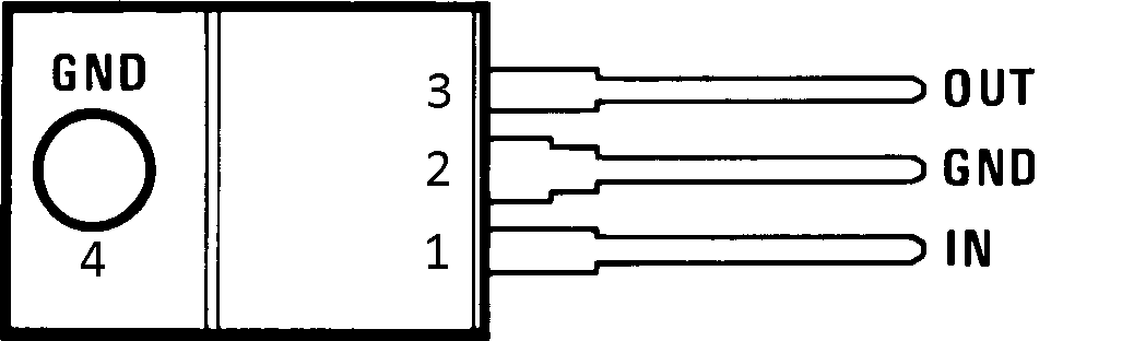
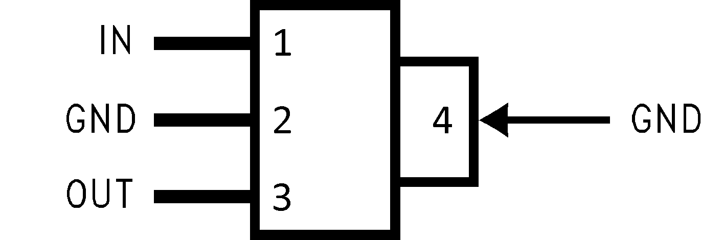
5 Pin Configuration and Functions
DDPAK/TO-263 (KTT) Package
3 Pins
Top View
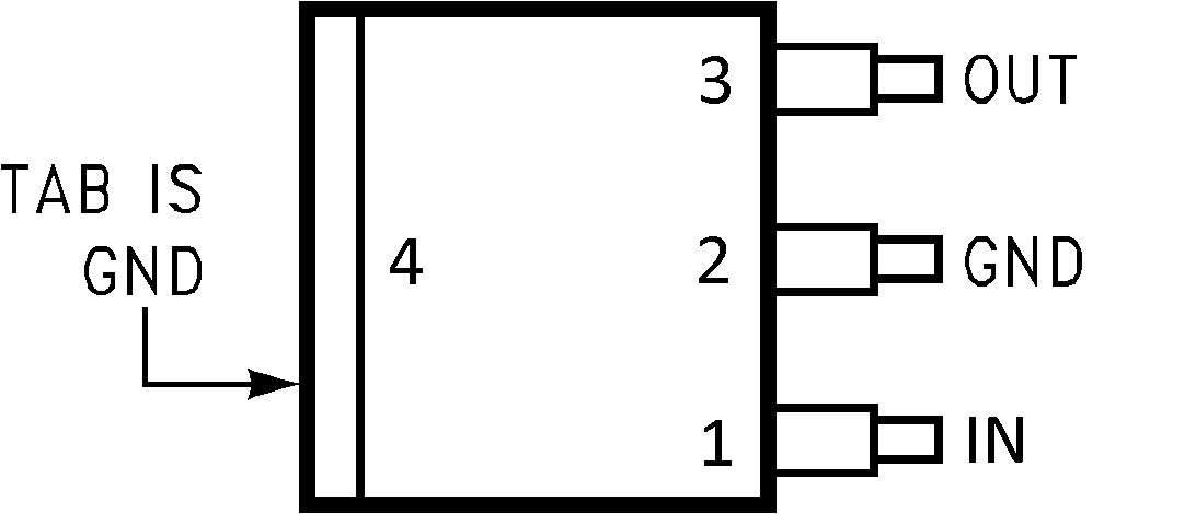
TO-220 (NDE) Package
4 Pins
Front View
SOT-223 (DCY) Package
3 Pins
Front View
DDPAK/TO-263 ( KTT) Package
Side View

WSON (NGN) Package
8 Pins
Top View
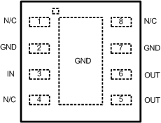
Pin 2 and pin 7 are fused to center DAP
Pin 5 and 6 need to be tied together on PCB board
Pin 5 and 6 need to be tied together on PCB board
Pin Functions
| PIN | I/O | DESCRIPTION | ||||
|---|---|---|---|---|---|---|
| NAME | NDE | KTT | DCY | NGN | ||
| IN | 1 | 1 | 1 | 3 | I | Unregulated input voltage. |
| GND | 2 | 2 | 2 | 2 | — | Ground |
| OUT | 3 | 3 | 3 | 5, 6 | O | Regulated output voltage. This pin requires an output capacitor to maintain stability. See Detailed Design Procedure for output capacitor details. |
| GND | 4 | 4 | 4 | 7 | — | Ground |
| N/C | — | — | — | 1, 4, 8 | — | No connection |