SLCS144E July 2004 – October 2014 LM317L
PRODUCTION DATA.
- 1 Features
- 2 Applications
- 3 Description
- 4 Simplified Schematic
- 5 Revision History
- 6 Pin Configuration and Functions
- 7 Specifications
- 8 Detailed Description
-
9 Application and Implementation
- 9.1 Application Information
- 9.2 Typical Application
- 9.3
General Configurations
- 9.3.1 Regulator Circuit With Improved Ripple Rejection
- 9.3.2 0-V to 30-V Regulator Circuit
- 9.3.3 Precision Current-Limiter Circuit
- 9.3.4 Tracking Preregulator Circuit
- 9.3.5 Slow-Turn On 15-V Regulator Circuit
- 9.3.6 50-mA Constant-Current Battery-Charger Circuit
- 9.3.7 Current-Limited 6-V Charger
- 9.3.8 High-Current Adjustable Regulator
- 10Power Supply Recommendations
- 11Layout
- 12Device and Documentation Support
- 13Mechanical, Packaging, and Orderable Information
パッケージ・オプション
デバイスごとのパッケージ図は、PDF版データシートをご参照ください。
メカニカル・データ(パッケージ|ピン)
- D|8
- PW|8
- PK|3
- LP|3
サーマルパッド・メカニカル・データ
- PK|3
発注情報
7 Specifications
7.1 Absolute Maximum Ratings(1)
over operating temperature range (unless otherwise noted)| MIN | MAX | UNIT | |||
|---|---|---|---|---|---|
| Vl – VO | Input-to-output differential voltage | 35 | V | ||
| TJ | Operating virtual-junction temperature | 150 | °C | ||
(1) Stresses beyond those listed under Absolute Maximum Ratings may cause permanent damage to the device. These are stress ratings only, and functional operation of the device at these or any other conditions beyond those indicated under Recommended Operating Conditions is not implied. Exposure to absolute-maximum-rated conditions for extended periods may affect device reliability.
7.2 Handling Ratings
| MIN | MAX | UNIT | |||
|---|---|---|---|---|---|
| Tstg | Storage temperature range | –65 | 150 | °C | |
| V(ESD) | Electrostatic discharge | Human body model (HBM), per ANSI/ESDA/JEDEC JS-001, all pins(1) | 0 | 3000 | V |
| Charged device model (CDM), per JEDEC specification JESD22-C101, all pins(2) | 0 | 2000 | |||
(1) JEDEC document JEP155 states that 500-V HBM allows safe manufacturing with a standard ESD control process.
(2) JEDEC document JEP157 states that 250-V CDM allows safe manufacturing with a standard ESD control process.
7.3 Recommended Operating Conditions
| MIN | MAX | UNIT | |||
|---|---|---|---|---|---|
| VO | Output voltage | 1.25 | 32 | V | |
| VI – VO | Input-to-output voltage differential | 2.5 | 32 | V | |
| IO | Output current | 2.5 | 100 | mA | |
| TJ | Operating virtual-junction temperature | LM317LC | 0 | 125 | °C |
| LM317LI | –40 | 125 | |||
7.4 Thermal Information
| THERMAL METRIC(1) | LM317L | UNIT | |||||
|---|---|---|---|---|---|---|---|
| D 8 PINS |
LP 3 PINS |
PK 3 PINS |
PW 8 PINS |
||||
| RθJA | Junction-to-ambient thermal resistance | 97.1 | 139.5 | 51.5 | 149.4 | °C/W | |
(1) For more information about traditional and new thermal metrics, see the IC Package Thermal Metrics application report (SPRA953).
7.5 Electrical Characteristics
over recommended operating virtual-junction temperature range (unless otherwise noted)| PARAMETER | TEST CONDITIONS(1) | MIN | TYP | MAX | UNIT | |
|---|---|---|---|---|---|---|
| Input voltage regulation(2) | VI – VO = 5 V to 35 V | TJ = 25°C | 0.01 | 0.02 | %V | |
| IO = 2.5 mA to 100 mA | 0.02 | 0.05 | ||||
| Ripple regulation | VO = 10 V, | f = 120 Hz | 65 | dB | ||
| VO = 10 V, 10-μF capacitor between ADJUSTMENT and ground |
66 | 80 | ||||
| Output voltage regulation | VI = 5 V to 35 V, TJ = 25°C, IO = 2.5 mA to 100 mA, |
VO ≤ 5 V | 25 | mV | ||
| VO ≥ 5 V | 5 | mV/V | ||||
| VI = 5 V to 35 V, IO = 2.5 mA to 100 mA |
VO ≤ 5 V | 50 | mV | |||
| VO ≥ 5 V | 10 | mV/V | ||||
| Output voltage change with temperature | TJ = 0°C to 125°C | 10 | mV/V | |||
| Output voltage long-term drift | After 1000 hours at TJ = 125°C and VI – VO = 35 V | 3 | 10 | mV/V | ||
| Output noise voltage | f = 10 Hz to 10 kHz, | TJ = 25°C | 30 | μV/V | ||
| Minimum output current to maintain regulation | VI – VO = 35 V | 1.5 | 2.5 | mA | ||
| Peak output current | VI – VO ≤ 35 V | 100 | 200 | mA | ||
| ADJUSTMENT current | 50 | 100 | μA | |||
| Change in ADJUSTMENT current | VI – VO = 2.5 V to 35 V, | IO = 2.5 mA to 100 mA | 0.2 | 5 | μA | |
| Reference voltage (output to ADJUSTMENT) | VI – VO = 5 V to 35 V, P ≤ rated dissipation |
IO = 2.5 mA to 100 mA, | 1.2 | 1.25 | 1.3 | V |
(1) Unless otherwise noted, these specifications apply for the following test conditions: VI – VO = 5 V and IO = 40 mA. Pulse-testing techniques must be used that maintain the junction temperature as close to the ambient temperature as possible. All characteristics are measured with a 0.1-μF capacitor across the input and a 1-μF capacitor across the output.
(2) Input voltage regulation is expressed here as the percentage change in output voltage per 1-V change at the input.
7.6 Typical Characteristics
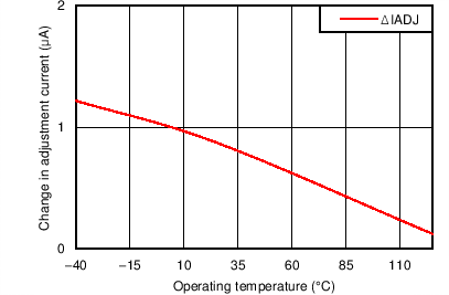 Figure 1. Change in Adjustment Current Over Temperature