SNVS846G June 2012 – November 2017 LM34925
PRODUCTION DATA.
- 1 Features
- 2 Applications
- 3 Description
- 4 Revision History
- 5 Pin Configuration and Functions
- 6 Specifications
-
7 Detailed Description
- 7.1 Overview
- 7.2 Functional Block Diagram
- 7.3
Feature Description
- 7.3.1 Control Overview
- 7.3.2 VCC Regulator
- 7.3.3 Regulation Comparator
- 7.3.4 Overvoltage Comparator
- 7.3.5 On-Time Generator
- 7.3.6 Current Limit
- 7.3.7 N-Channel Buck Switch and Driver
- 7.3.8 Synchronous Rectifier
- 7.3.9 Undervoltage Detector
- 7.3.10 Thermal Protection
- 7.3.11 Ripple Configuration
- 7.3.12 Soft Start
- 7.4 Device Functional Modes
-
8 Application and Implementation
- 8.1 Application Information
- 8.2
Typical Application
- 8.2.1
Application Circuit: 20-V to 95-V Input and 10-V, 100-mA Output Isolated Fly-Buck Converter
- 8.2.1.1 Design Requirements
- 8.2.1.2
Detailed Design Procedure
- 8.2.1.2.1 Transformer Turns Ratio
- 8.2.1.2.2 Total IOUT
- 8.2.1.2.3 RFB1, RFB2
- 8.2.1.2.4 Frequency Selection
- 8.2.1.2.5 Transformer Selection
- 8.2.1.2.6 Primary Output Capacitor
- 8.2.1.2.7 Secondary Output Capacitor
- 8.2.1.2.8 Type III Feedback Ripple Circuit
- 8.2.1.2.9 Secondary Diode
- 8.2.1.2.10 VCC and Bootstrap Capacitor
- 8.2.1.2.11 Input Capacitor
- 8.2.1.2.12 UVLO Resistors
- 8.2.1.2.13 VCC Diode
- 8.2.2 Application Curves
- 8.2.1
Application Circuit: 20-V to 95-V Input and 10-V, 100-mA Output Isolated Fly-Buck Converter
- 9 Power Supply Recommendations
- 10Layout
- 11Device and Documentation Support
- 12Mechanical, Packaging, and Orderable Information
パッケージ・オプション
メカニカル・データ(パッケージ|ピン)
サーマルパッド・メカニカル・データ
- DDA|8
発注情報
8 Application and Implementation
NOTE
Information in the following applications sections is not part of the TI component specification, and TI does not warrant its accuracy or completeness. TI’s customers are responsible for determining suitability of components for their purposes. Customers should validate and test their design implementation to confirm system functionality.
8.1 Application Information
The LM34925 device is step-down dc-to-dc converter. The device is typically used to convert a higher dc voltage to a lower dc voltage with a maximum available output current of 100 mA. Use the following design procedure to select component values for the LM34925 device. Alternately, use the WEBENCH® software to generate a complete design. The WEBENCH software uses an iterative design procedure and accesses a comprehensive database of components when generating a design. This section presents a simplified discussion of the design process.
8.2 Typical Application
8.2.1 Application Circuit: 20-V to 95-V Input and 10-V, 100-mA Output Isolated Fly-Buck™ Converter
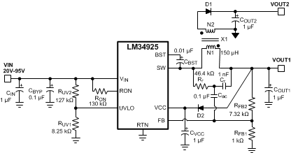 Figure 12. Isolated Fly-Buck Converter Using LM34925
8.2.1.1 Design Requirements
Selection of external components is illustrated through a design example. The design example specifications are shown in Table 3.
Table 3. Buck Converter Design Specifications
| DESIGN PARAMETERS | VALUE |
|---|---|
| Input Voltage Range | 20 V to 95 V |
| Primary Output Voltage | 10 V |
| Secondary (Isolated) Output Voltage | 9.5 V |
| Maximum Output Current (Primary + Secondary) | 100 mA |
| Maximum Power Output | 1 W |
| Nominal Switching Frequency | 750 kHz |
8.2.1.2 Detailed Design Procedure
8.2.1.2.1 Transformer Turns Ratio
The transformer turns ratio is selected based on the ratio of the primary output voltage to the secondary (isolated) output voltage. In this design example, the two outputs are nearly equal and a 1:1 turns ratio transformer is selected. Therefore, N2 / N1 = 1. If the secondary (isolated) output voltage is significantly higher or lower than the primary output voltage, a turns ratio less than or greater than 1 is recommended. The primary output voltage is normally selected based on the input voltage range such that the duty cycle of the converter does not exceed 50% at the minimum input voltage. This condition is satisfied if VOUT1 < VIN_MIN / 2.
8.2.1.2.2 Total IOUT
The total primary referred load current is calculated by multiplying the isolated output load(s) by the turns ratio of the transformer as shown in Equation 7.

8.2.1.2.3 RFB1, RFB2
The feedback resistors are selected to set the primary output voltage. The selected value for RFB1 is 1 kΩ. RFB2 can be calculated using the following equations to set VOUT1 to the specified value of 10 V. A standard resistor value of 7.32 kΩ is selected for RFB2.


8.2.1.2.4 Frequency Selection
Equation 1 is used to calculate the value of RON required to achieve the desired switching frequency.

Where K = 9 × 10–11 For VOUT1 of 10 V and fSW of 750 kHz, the calculated value of RON is 148 kΩ. A lower value of 130 kΩ is selected for this design to allow for second order effects at high switching frequency that are not included in Equation 1.
8.2.1.2.5 Transformer Selection
A coupled inductor or a flyback-type transformer is required for this topology. Energy is transferred from primary to secondary when the low-side synchronous switch of the buck converter is conducting.
The maximum inductor primary ripple current that can be tolerated without exceeding the buck switch peak current limit threshold (0.15 A minimum) is given by Equation 11.

Using the maximum peak-to-peak inductor ripple current ΔIL1 from Equation 11, the minimum inductor value is given by Equation 12.

A higher value of 150 µH is selected to insure the high-side switch current does not exceed the minimum peak current limit threshold.
8.2.1.2.6 Primary Output Capacitor
In a conventional buck converter the output ripple voltage is calculated as shown in Equation 13.

To limit the primary output ripple voltage ΔVOUT1 to approximately 50 mV, an output capacitor COUT1 of 0.33 µF is required.
Figure 13 shows the primary winding current waveform (IL1) of a Fly-Buck converter. The reflected secondary winding current adds to the primary winding current during the buck switch off-time. Because of this increased current, the output voltage ripple is not the same as in conventional buck converter. The output capacitor value calculated in Equation 13 should be used as the starting point. Optimization of output capacitance over the entire line and load range must be done experimentally. If the majority of the load current is drawn from the secondary isolated output, a better approximation of the primary output voltage ripple is given by Equation 14.

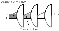 Figure 13. Current Waveforms for COUT1 Ripple Calculation
A standard 1-µF, 25-V capacitor is selected for this design. If lower output voltage ripple is required, a higher value should be selected for COUT1 and/or COUT2.
8.2.1.2.7 Secondary Output Capacitor
A simplified waveform for secondary output current (IOUT2) is shown in Figure 14.
 Figure 14. Secondary Current Waveforms for COUT2 Ripple Calculation
The secondary output current (IOUT2) is sourced by COUT2 during on-time of the buck switch, TON. Ignoring the current transition times in the secondary winding, the secondary output capacitor ripple voltage can be calculated using Equation 15.

For a 1:1 transformer turns ratio, the primary and secondary voltage ripple equations are identical. Therefore, COUT2 is chosen to be equal to COUT1 (1 µF) to achieve comparable ripple voltages on primary and secondary outputs.
If lower output voltage ripple is required, a higher value should be selected for COUT1 and/or COUT2.
8.2.1.2.8 Type III Feedback Ripple Circuit
Type III ripple circuit as described in Ripple Configuration is required for the Fly-Buck topology. Type I and Type II ripple circuits use series resistance and the triangular inductor ripple current to generate ripple at VOUT and the FB pin. The primary ripple current of a Fly-Buck is the combination or primary and reflected secondary currents as illustrated in Figure 13. In the Fly-Buck topology, Type I and Type II ripple circuits suffer from large jitter as the reflected load current affects the feedback ripple.
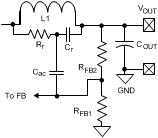 Figure 15. Type III Ripple Circuit
Selecting the Type III ripple components using the equations from Ripple Configuration will guarantee that the FB pin ripple is be greater than the capacitive ripple from the primary output capacitor COUT1. The feedback ripple component values are chosen as shown in Equation 16.

The calculated value for Rr is 66 kΩ. This value provides the minimum ripple for stable operation. A smaller resistance should be selected to allow for variations in TON, COUT1 and other components. For this design, Rr value of 46.4 kΩ is selected.
8.2.1.2.9 Secondary Diode
The reverse voltage across secondary-rectifier diode D1 when the high-side buck switch is off can be calculated using Equation 17.

For a VIN_MAX of 95 V and the 1:1 turns ratio of this design, a 100-V Schottky is selected.
8.2.1.2.10 VCC and Bootstrap Capacitor
A 1-µF capacitor of 16-V or higher rating is recommended for the VCC regulator bypass capacitor.
A good value for the BST pin bootstrap capacitor is 0.01-µF with a 16-V or higher rating.
8.2.1.2.11 Input Capacitor
The input capacitor is typically a combination of a smaller bypass capacitor located near the regulator IC and a larger bulk capacitor. The total input capacitance should be large enough to limit the input voltage ripple to a desired amplitude. For input ripple voltage ΔVIN, CIN can be calculated using Equation 18.

Choosing a ΔVIN of 0.5 V gives a minimum CIN of 0.067 μF. A standard value of 0.1 μF is selected for CBYP in this design. A bulk capacitor of higher value reduces voltage spikes due to parasitic inductance between the power source to the converter. A standard value of 1 μF is selected for CIN in this design. The voltage ratings of the two input capacitors should be greater than the maximum input voltage under all conditions.
8.2.1.2.12 UVLO Resistors
UVLO resistors RUV1 and RUV2 set the undervoltage lockout threshold and hysteresis according to Equation 19 and Equation 20.


Where IHYS = 20 μA, typical.
For a UVLO hysteresis of 2.5 V and UVLO rising threshold of 20 V, Equation 19 and Equation 20 require RUV1 of 8.25 kΩ and RUV2 of 127 kΩ and these values are selected for this design example.
8.2.1.2.13 VCC Diode
Diode D2 is an optional diode connected between VOUT1 and the VCC regulator output pin. When VOUT1 is more than one diode drop greater than the VCC voltage, the VCC bias current is supplied from VOUT1. This results in reduced power losses in the internal VCC regulator which improves converter efficiency. VOUT1 must be set to a voltage at least one diode drop higher than 8.55 V (the maximum VCC voltage) if D2 is used to supply bias current.
8.2.2 Application Curves
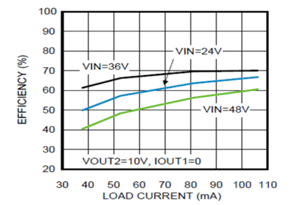
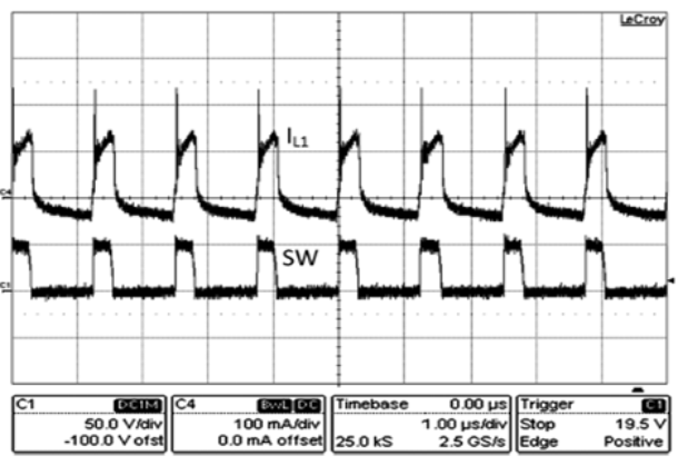
(VIN = 48 V, IOUT1 = 0 mA, IOUT2 = 100 mA)