SNVS846G June 2012 – November 2017 LM34925
PRODUCTION DATA.
- 1 Features
- 2 Applications
- 3 Description
- 4 Revision History
- 5 Pin Configuration and Functions
- 6 Specifications
-
7 Detailed Description
- 7.1 Overview
- 7.2 Functional Block Diagram
- 7.3
Feature Description
- 7.3.1 Control Overview
- 7.3.2 VCC Regulator
- 7.3.3 Regulation Comparator
- 7.3.4 Overvoltage Comparator
- 7.3.5 On-Time Generator
- 7.3.6 Current Limit
- 7.3.7 N-Channel Buck Switch and Driver
- 7.3.8 Synchronous Rectifier
- 7.3.9 Undervoltage Detector
- 7.3.10 Thermal Protection
- 7.3.11 Ripple Configuration
- 7.3.12 Soft Start
- 7.4 Device Functional Modes
-
8 Application and Implementation
- 8.1 Application Information
- 8.2
Typical Application
- 8.2.1
Application Circuit: 20-V to 95-V Input and 10-V, 100-mA Output Isolated Fly-Buck Converter
- 8.2.1.1 Design Requirements
- 8.2.1.2
Detailed Design Procedure
- 8.2.1.2.1 Transformer Turns Ratio
- 8.2.1.2.2 Total IOUT
- 8.2.1.2.3 RFB1, RFB2
- 8.2.1.2.4 Frequency Selection
- 8.2.1.2.5 Transformer Selection
- 8.2.1.2.6 Primary Output Capacitor
- 8.2.1.2.7 Secondary Output Capacitor
- 8.2.1.2.8 Type III Feedback Ripple Circuit
- 8.2.1.2.9 Secondary Diode
- 8.2.1.2.10 VCC and Bootstrap Capacitor
- 8.2.1.2.11 Input Capacitor
- 8.2.1.2.12 UVLO Resistors
- 8.2.1.2.13 VCC Diode
- 8.2.2 Application Curves
- 8.2.1
Application Circuit: 20-V to 95-V Input and 10-V, 100-mA Output Isolated Fly-Buck Converter
- 9 Power Supply Recommendations
- 10Layout
- 11Device and Documentation Support
- 12Mechanical, Packaging, and Orderable Information
パッケージ・オプション
メカニカル・データ(パッケージ|ピン)
サーマルパッド・メカニカル・データ
- DDA|8
発注情報
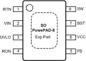
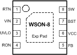
5 Pin Configuration and Functions
DDA Package
8-Pin SO PowerPAD
Top View

NGU Package
8-Pin WSON With Exposed Thermal Pad
Top View

Pin Functions
| PIN | I/O | DESCRIPTION | APPLICATION INFORMATION | |
|---|---|---|---|---|
| NO. | NAME | |||
| 1 | RTN | — | Ground | Ground connection of the integrated circuit. |
| 2 | VIN | I | Input Voltage | Operating input range is 7.5 V to 100 V. |
| 3 | UVLO | I | Input Pin of Undervoltage Comparator | Resistor divider from VIN to UVLO to GND programs the undervoltage detection threshold. An internal current source is enabled when UVLO is above 1.225 V to provide hysteresis. When UVLO pin is pulled below 0.66 V externally, the parts goes in shutdown mode. |
| 4 | RON | I | On-Time Control | A resistor between this pin and VIN sets the switch on-time as a function of VIN. Minimum recommended on-time is 100ns at max input voltage. |
| 5 | FB | I | Feedback | This pin is connected to the inverting input of the internal regulation comparator. The regulation level is 1.225 V. |
| 6 | VCC | O | Output from the Internal High Voltage Series Pass Regulator. Regulated at 7.6 V. |
The internal VCC regulator provides bias supply for the gate drivers and other internal circuitry. A 1-μF decoupling capacitor is recommended. |
| 7 | BST | I | Bootstrap Capacitor | An external capacitor is required between the BST and SW pins (0.01 μF ceramic). The BST pin capacitor is charged by the VCC regulator through an internal diode when the SW pin is low. |
| 8 | SW | O | Switching Node | Power switching node. Connect to the output inductor and bootstrap capacitor. |
| — | EP | — | Exposed Pad | Exposed pad must be connected to RTN pin. Connect to system ground plane on application board for reduced thermal resistance. |