SNVS847F June 2012 – November 2017 LM34926
PRODUCTION DATA.
- 1 Features
- 2 Applications
- 3 Description
- 4 Revision History
- 5 Pin Configuration and Functions
- 6 Specifications
-
7 Detailed Description
- 7.1 Overview
- 7.2 Functional Block Diagram
- 7.3
Feature Description
- 7.3.1 Control Overview
- 7.3.2 VCC Regulator
- 7.3.3 Regulation Comparator
- 7.3.4 Overvoltage Comparator
- 7.3.5 On-Time Generator
- 7.3.6 Current Limit
- 7.3.7 N-Channel Buck Switch and Driver
- 7.3.8 Synchronous Rectifier
- 7.3.9 Undervoltage Detector
- 7.3.10 Thermal Protection
- 7.3.11 Ripple Configuration
- 7.3.12 Soft Start
- 7.4 Device Functional Modes
-
8 Application and Implementation
- 8.1 Application Information
- 8.2
Typical Application
- 8.2.1 Design Requirements
- 8.2.2
Detailed Design Procedure
- 8.2.2.1 Custom Design With WEBENCH® Tools
- 8.2.2.2 Transformer Turns Ratio
- 8.2.2.3 Total IOUT
- 8.2.2.4 RFB1, RFB2
- 8.2.2.5 Frequency Selection
- 8.2.2.6 Transformer Selection
- 8.2.2.7 Primary Output Capacitor
- 8.2.2.8 Secondary Output Capacitor
- 8.2.2.9 Type III Feedback Ripple Circuit
- 8.2.2.10 Secondary Diode
- 8.2.2.11 VCC and Bootstrap Capacitor
- 8.2.2.12 Input Capacitor
- 8.2.2.13 UVLO Resistors
- 8.2.2.14 VCC Diode
- 8.2.3 Application Curves
- 9 Power Supply Recommendations
- 10Layout
- 11Device and Documentation Support
- 12Mechanical, Packaging, and Orderable Information
パッケージ・オプション
メカニカル・データ(パッケージ|ピン)
サーマルパッド・メカニカル・データ
- DDA|8
発注情報
7 Detailed Description
7.1 Overview
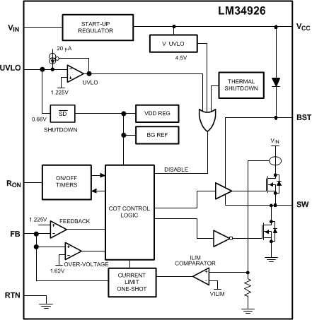
The LM34926 step-down switching regulator features all the functions needed to implement a low-cost, efficient, isolated bias supply. This high-voltage regulator contains 100-V, N-channel buck and synchronous switches, is easy to implement, and is provided in thermally enhanced SO PowerPAD-8 and WSON-8 packages. The regulator operation is based on a constant on-time control scheme using an on-time inversely proportional to VIN. This control scheme does not require loop compensation. Current limit is implemented with forced off-time inversely proportional to VOUT. This scheme ensures short circuit protection while providing minimum foldback. The simplified block diagram of the LM34926 device is shown in Functional Block Diagram.
The LM34926 device can be applied in numerous applications to efficiently regulate down higher voltages. This regulator is well suited for 48-V telecom and automotive power bus ranges. Protection features include: thermal shutdown, undervoltage lockout, minimum forced off-time, and an intelligent current limit.
7.2 Functional Block Diagram
7.3 Feature Description
7.3.1 Control Overview
The LM34926 regulator employs a control principle based on a comparator and a one-shot on-timer, with the output voltage feedback (FB) compared to an internal reference (1.225 V). If the FB voltage is below the reference the internal buck switch is switched on for the one-shot timer period, which is a function of the input voltage and the programming resistor (RT). Following the on-time the switch remains off until the FB voltage falls below the reference, and the forced minimum off-time has expired. When the FB pin voltage falls below the reference and the off-time one-shot period expires, the buck switch is then turned on for another on-time one-shot period. This continues until regulation is achieved and the FB voltage is approximately equal to 1.225 V (typical).
In a synchronous buck converter, the low-side (sync) FET is on when the high-side (buck) FET is off. The inductor current ramps up when the high-side switch is on and ramps down when the high-side switch is off. There is no diode emulation feature in this IC, and therefore, the inductor current may ramp in the negative direction at light load. This causes the converter to operate in continuous conduction mode (CCM) regardless of the output loading. The operating frequency remains relatively constant with load and line variations. The operating frequency can be determined from Equation 1.

where
The output voltage (VOUT) is set by two external resistors (RFB1, RFB2). The regulated output voltage is determined from Equation 2.

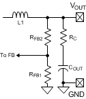
This regulator regulates the output voltage based on ripple voltage at the feedback input, requiring a minimum amount of ESR for the output capacitor (COUT). A minimum of 25 mV of ripple voltage at the feedback pin (FB) is required for the LM34926 device. In cases where the capacitor ESR is too small, additional series resistance may be required (RC in Figure 9).
For applications where lower output voltage ripple is required the output can be taken directly from a low ESR output capacitor, as shown in Figure 9. However, RC slightly degrades the load regulation.
 Figure 9. Low Ripple Output Configuration
7.3.2 VCC Regulator
The LM34926 device contains an internal high-voltage linear regulator with a nominal output of 7.6 V. The input pin (VIN) can be connected directly to the line voltages up to 100 V. The VCC regulator is internally current limited to 30 mA. The regulator sources current into the external capacitor at VCC. This regulator supplies current to internal circuit blocks including the synchronous MOSFET driver and the logic circuits. When the voltage on the VCC pin reaches the UVLO threshold of 4.5 V, the IC is enabled.
The VCC regulator contains an internal diode connection to the BST pin to replenish the charge in the gate drive boot capacitor when the SW pin is low.
At high input voltages, the power dissipated in the high-voltage regulator is significant and can limit the overall achievable output power. As an example, with the input at 48 V and switching at high frequency, the VCC regulator may supply up to 7 mA of current resulting in 48 V × 7 mA = 336 mW of power dissipation. If the VCC voltage is driven externally by an alternate voltage source, from 8.55 V to 13 V, the internal regulator is disabled. This reduces the power dissipation in the IC.
7.3.3 Regulation Comparator
The feedback voltage at FB is compared to an internal 1.225 V reference. In normal operation, when the output voltage is in regulation, an on-time period is initiated when the voltage at FB falls below 1.225 V. The high-side switch stays on for the on-time, causing the FB voltage to rise above 1.225 V. After the on-time period, the high-side switch stays off until the FB voltage again falls below 1.225 V. During start-up, the FB voltage is below 1.225 V at the end of each on-time, causing the high-side switch to turn on immediately after the minimum forced off-time of 144 ns. The high-side switch can be turned off before the on-time is complete if peak current in the inductor reaches the current limit threshold.
7.3.4 Overvoltage Comparator
The feedback voltage at FB is compared to an internal 1.62 V reference. If the voltage at FB rises above 1.62-V the on-time pulse is immediately terminated. This condition can occur if the input voltage and/or the output load changes suddenly. The high-side switch will not turn on again until the voltage at FB falls below 1.225 V.
7.3.5 On-Time Generator
The on-time for the LM34926 device is determined by the RON resistor, and is inversely proportional to the input voltage (VIN), resulting in a nearly constant frequency as VIN is varied over its range. The on-time equation for the LM34926 is determined be Equation 3.

See Figure 5. RON should be selected for a minimum on-time (at maximum VIN) greater than 100 ns, for proper operation. This requirement limits the maximum frequency for each application.
7.3.6 Current Limit
The LM34926 device contains an intelligent current limit off-timer. If the current in the buck switch exceeds
575 mA, the present cycle is immediately terminated, and a non-resetable off-timer is initiated. The length of off-time is controlled by the FB voltage and the input voltage VIN. As an example, when FB = 0 V and VIN = 48 V, a maximum off-time is set to 16 μs. This condition occurs when the output is shorted, and during the initial part of start-up. This amount of time ensures safe short circuit operation up to the maximum input voltage of
100 V.
In cases of overload where the FB voltage is above zero volts (not a short circuit) the current limit off-time is reduced. Reducing the off-time during less severe overloads reduces the amount of foldback, recovery time, and start-up time. The off-time is calculated from Equation 4.

The current limit protection feature is peak limited, the maximum average output will be less than the peak.
7.3.7 N-Channel Buck Switch and Driver
The LM34926 device integrates an N-channel buck switch and associated floating high voltage gate driver. The gate driver circuit works in conjunction with an external bootstrap capacitor and an internal high-voltage diode. A 0.01-uF ceramic capacitor connected between the BST and SW pins provides the voltage to the driver during the on-time. During each off-time, the SW pin is at approximately 0 V, and the bootstrap capacitor charges from VCC through the internal diode. The minimum off-timer, set to 144 ns, ensures a minimum time each cycle to recharge the bootstrap capacitor.
7.3.8 Synchronous Rectifier
The LM34926 device provides an internal synchronous N-Channel MOSFET rectifier. This MOSFET provides a path for the inductor current to flow when the high-side MOSFET is turned off.
The synchronous rectifier has no diode emulation mode, and is designed to keep the regulator in continuous conduction mode even during light loads which would otherwise result in discontinuous operation. This feature specifically allows the user to design a secondary regulator using a transformer winding off the main inductor to generate the alternate regulated output voltage.
7.3.9 Undervoltage Detector
The LM34926 device contains a dual-level UVLO circuit. A summary of threshold voltages and operational states is provided in Device Functional Modes. When the UVLO pin voltage is below 0.66 V, the controller is in a low current shutdown mode. When the UVLO pin voltage is greater than 0.66 V but less than 1.225 V, the controller is in standby mode. In standby mode the VCC bias regulator is active while the regulator output is disabled. When the VCC pin exceeds the VCC undervoltage thresholds and the UVLO pin voltage is greater than 1.225 V, normal operation begins. An external set-point voltage divider from VIN to GND can be used to set the minimum operating voltage of the regulator.
UVLO hysteresis is accomplished with an internal 20-μA current source that is switched on or off into the impedance of the set-point divider. When the UVLO threshold is exceeded, the current source is activated to quickly raise the voltage at the UVLO pin. The hysteresis is equal to the value of this current times the resistance RUV2.
If the UVLO pin is wired directly to the VIN pin, the regulator will begin operation once the VCC undervoltage is satisfied.
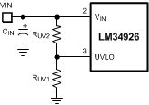 Figure 10. UVLO Resistor Setting
7.3.10 Thermal Protection
The LM34926 device should be operated so the junction temperature does not exceed 150°C during normal operation. An internal Thermal Shutdown circuit is provided to protect the LM34926 device in the event of a higher than normal junction temperature. When activated, typically at 165°C, the controller is forced into a low-power reset state, disabling the buck switch and the VCC regulator. This feature prevents catastrophic failures from accidental device overheating. When the junction temperature falls below 145°C (typical hysteresis = 20°C), the VCC regulator is enabled, and normal operation is resumed.
7.3.11 Ripple Configuration
LM34926 uses constant on-time (COT) control scheme, in which the on-time is terminated by an on-timer, and the off-time is terminated by the feedback voltage (VFB) falling below the reference voltage (VREF). Therefore, for stable operation, the feedback voltage must decrease monotonically, in phase with the inductor current during the off-time. Furthermore this change in feedback voltage (ΔVFB) during off-time must be large enough to suppress any noise component present at the feedback node.
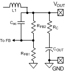
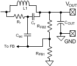
Table 1 shows three different methods for generating appropriate voltage ripple at the feedback node. Type 1 and Type 2 ripple circuits couple the ripple at the output of the converter to the feedback node (FB). The output voltage ripple has two components:
- Capacitive ripple caused by the inductor current ripple charging and discharging the output capacitor.
- Resistive ripple caused by the inductor current ripple flowing through the ESR of the output capacitor.
The capacitive ripple is not in phase with the inductor current. As a result, the capacitive ripple does not decrease monotonically during the off-time. The resistive ripple is in phase with the inductor current and decreases monotonically during off-time. The resistive ripple must exceed the capacitive ripple at the output node (VOUT) for stable operation. If this condition is not satisfied, unstable switching behavior is observed in COT converters, with multiple on-time bursts in close succession followed by a long off-time.
Type 3 ripple method uses Rr and Cr and the switch node (SW) voltage to generate a triangular ramp. This triangular ramp is AC-coupled using Cac to the feedback node (FB). Because this circuit does not use the output voltage ripple, it is ideally suited for applications where low output voltage ripple is required. See AN-1481 Controlling Output Ripple and Achieving ESR Independence in Constant On-Time (COT) Regulator Designs (SNVA166) for more details for each ripple generation method.
Table 1. Ripple Configuration
| TYPE 1 LOWEST COST CONFIGURATION |
TYPE 2 REDUCED RIPPLE CONFIGURATION |
TYPE 3 MINIMUM RIPPLE CONFIGURATION |
|---|---|---|
 |
 |
 |
 |
 |

|
7.3.12 Soft Start
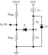
A soft-start feature can be implemented with the LM34926 device using an external circuit. As shown in Figure 11, the soft-start circuit consists of one capacitor C1, two resistors R1 and R2, and a diode D. During the initial start-up, the VCC voltage is established before the VOUT voltage. Capacitor C1 is discharged and diode D is thereby forward biased to pull up the FB voltage. The FB voltage exceeds the reference voltage (1.225 V) and switching is therefore disabled. As capacitor C1 charges, the voltage at node B gradually decreases and switching commences. VOUT will gradually rise to maintain the FB voltage at the reference voltage. Once the voltage at node B is less than a diode drop above the FB voltage, the soft-start sequence is finished and D is reverse-biased.
During the initial part of the start-up, the FB voltage can be approximated as shown in Equation 5. The effect of R1 has been ignored to simplify the calculation.

C1 is charged after the first start up. Diode D1 is optional and can be added to discharge C1 when the input voltage experiences a momentary drop to initialize the soft-start sequence.
To achieve the desired soft start, the following design guidance is recommended:
- R2 is selected so that VFB is higher than 1.225 V for a VCC of 4.5 V, but is lower than 5 V when VCC is 8.55 V. If an external VCC is used, VFB should not exceed 5 V at maximum VCC.
- C1 is selected to achieve the desired start-up time which can be determined from .
- R1 is used to maintain the node B voltage at zero after the soft start is finished. A value larger than the feedback resistor divider is preferred. The effect of resistor R1 is ignored.

Using the component values shown in Figure 12, selecting C1 = 1 uF, R2 = 1 kΩ, R1 = 30 kΩ results in a soft-start time of about 2 ms.
7.4 Device Functional Modes
The UVLO pin controls the operating mode of the LM34926 device (see Table 2 for the detailed functional states).
Table 2. UVLO Mode
| UVLO | VCC | MODE | DESCRIPTION |
|---|---|---|---|
| < 0.66 V | Disabled | Shutdown | VCC regulator disabled. Switching disabled. |
| 0.66 V — 1.225 V | Enabled | Standby | VCC regulator enabled. Switching disabled. |
| > 1.225 V | VCC < 4.5 V | Standby | VCC regulator enabled. Switching disabled. |
| VCC > 4.5 V | Operating | VCC enabled. Switching enabled. |
