SNVS974B April   2013  – October 2015 LM3630A

PRODUCTION DATA.  

  1. Features
  2. Applications
  3. Description
  4. Revision History
  5. Pin Configuration and Functions
  6. Specifications
    1. 6.1 Absolute Maximum Ratings
    2. 6.2 ESD Ratings
    3. 6.3 Recommended Operating Conditions
    4. 6.4 Thermal Information
    5. 6.5 Electrical Characteristics
    6. 6.6 I2C-Compatible Timing Requirements (SCL, SDA)
    7. 6.7 Typical Characteristics
  7. Detailed Description
    1. 7.1 Overview
    2. 7.2 Functional Block Diagram
    3. 7.3 Feature Description
      1. 7.3.1 Operation
        1. 7.3.1.1  Control Bank Mapping
        2. 7.3.1.2  PWM Input Polaritiy
        3. 7.3.1.3  HWEN Input
        4. 7.3.1.4  SEL Input
        5. 7.3.1.5  INTN Output
        6. 7.3.1.6  Boost Converter
        7. 7.3.1.7  Boost Switching Frequency Select
        8. 7.3.1.8  Adaptive Headroom
        9. 7.3.1.9  Current Sinks
        10. 7.3.1.10 Current String Biasing
        11. 7.3.1.11 Full-Scale LED Current
        12. 7.3.1.12 Brightness Register
        13. 7.3.1.13 Exponential Mapping
        14. 7.3.1.14 Linear Mapping
      2. 7.3.2 Test Features
        1. 7.3.2.1 Open LED String (LED1 And LED2)
        2. 7.3.2.2 Shorted LED String
        3. 7.3.2.3 Overvoltage Protection (Manufacturing Fault Detection and Shutdown)
      3. 7.3.3 Fault Flags/Protection Features
        1. 7.3.3.1 Overvoltage Protection (Inductive Boost Operation)
        2. 7.3.3.2 Current Limit
        3. 7.3.3.3 Thermal Shutdown
      4. 7.3.4 Initialization Timing
        1. 7.3.4.1 Initialization Timing With HWEN Tied to VIN
        2. 7.3.4.2 Initialization Timing With HWEN Driven by GPIO
        3. 7.3.4.3 Initialization After Software Reset
    4. 7.4 Device Functional Modes
      1. 7.4.1 LED Current Ramping
        1. 7.4.1.1 Start-Up/Shutdown Ramp
        2. 7.4.1.2 Run-Time Ramp
      2. 7.4.2 PWM Operation
        1. 7.4.2.1 PWM Input
        2. 7.4.2.2 PWM Input Frequency
        3. 7.4.2.3 Recommended Settings
        4. 7.4.2.4 Adjustments to PWM Sampler
          1. 7.4.2.4.1 Filter Strength, Register 50h Bits [1:0]
          2. 7.4.2.4.2 Hysteresis 1 Bit, Register 05h, Bit 7
          3. 7.4.2.4.3 Lower Bound Disable, Register 05h, Bit 6
        5. 7.4.2.5 Minimum TON Pulse Width
    5. 7.5 Programming
      1. 7.5.1 I2C-Compatible Interface
        1. 7.5.1.1 Data Validity
        2. 7.5.1.2 Start and Stop Conditions
        3. 7.5.1.3 Transferring Data
    6. 7.6 Register Maps
      1. 7.6.1 LM3630A I2C Register Map
      2. 7.6.2 Register Descriptions
  8. Application and Implementation
    1. 8.1 Application Information
    2. 8.2 Typical Application
      1. 8.2.1 Design Requirements
      2. 8.2.2 Detailed Design Procedure
        1. 8.2.2.1 Inductor Selection
        2. 8.2.2.2 Maximum Power Output
      3. 8.2.3 Application Curves
    3. 8.3 Initialization Setup
      1. 8.3.1 Recommended Initialization Sequence
  9. Power Supply Recommendations
  10. 10Layout
    1. 10.1 Layout Guidelines
      1. 10.1.1 Output Capacitor Placement
      2. 10.1.2 Schottky Diode Placement
      3. 10.1.3 Inductor Placement
      4. 10.1.4 Input Capacitor Selection and Placement
    2. 10.2 Layout Example
  11. 11Device and Documentation Support
    1. 11.1 Device Support
      1. 11.1.1 Third-Party Products Disclaimer
    2. 11.2 Documentation Support
      1. 11.2.1 Related Documentation
    3. 11.3 Community Resources
    4. 11.4 Trademarks
    5. 11.5 Electrostatic Discharge Caution
    6. 11.6 Glossary
  12. 12Mechanical, Packaging, and Orderable Information

パッケージ・オプション

メカニカル・データ(パッケージ|ピン)
サーマルパッド・メカニカル・データ
発注情報

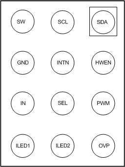
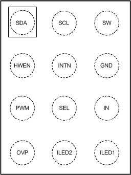
5 Pin Configuration and Functions

YFQ Package
12-Pin DSBGA
Top View
LM3630A package_top.gif
YFQ Package
12-Pin DSBGA
Bottom View
LM3630A package_bottom.gif

Pin Functions

PIN TYPE DESCRIPTION
NO. NAME
A1 SDA Input/Output Serial data connection for I2C-compatible interface
A2 SCL Input Serial clock connection for I2C-compatible interface
A3 SW PWR Inductor connection, diode anode connection, and drain connection for internal NFET. Connect the inductor and diode as close as possible to SW to reduce inductance and capacitive coupling to nearby traces.
B1 HWEN Input Logic high hardware enable
B2 INTN Output Interrupt output for fault status change. Open drain active low signal.
B3 GND GND Ground
C1 PWM Input External PWM brightness control input
C2 SEL Input Selects I2C-compatible address. Ground selects 7-bit address 36h. VIN selects address 38h.
C3 IN Input Input voltage connection. Connect a 2.3-V to 5.5-V supply to IN and bypass to GND with a 2.2-µF or greater ceramic capacitor.
D1 OVP Input Output voltage sense connection for overvoltage sensing. Connect OVP to the positive terminal of the output capacitor.
D2 ILED2 Input Input terminal to internal current sink 2.
D3 ILED1 Input Input terminal to internal current sink 1.