SNVS974B April 2013 – October 2015 LM3630A
PRODUCTION DATA.
- 1 Features
- 2 Applications
- 3 Description
- 4 Revision History
- 5 Pin Configuration and Functions
- 6 Specifications
-
7 Detailed Description
- 7.1 Overview
- 7.2 Functional Block Diagram
- 7.3
Feature Description
- 7.3.1
Operation
- 7.3.1.1 Control Bank Mapping
- 7.3.1.2 PWM Input Polaritiy
- 7.3.1.3 HWEN Input
- 7.3.1.4 SEL Input
- 7.3.1.5 INTN Output
- 7.3.1.6 Boost Converter
- 7.3.1.7 Boost Switching Frequency Select
- 7.3.1.8 Adaptive Headroom
- 7.3.1.9 Current Sinks
- 7.3.1.10 Current String Biasing
- 7.3.1.11 Full-Scale LED Current
- 7.3.1.12 Brightness Register
- 7.3.1.13 Exponential Mapping
- 7.3.1.14 Linear Mapping
- 7.3.2 Test Features
- 7.3.3 Fault Flags/Protection Features
- 7.3.4 Initialization Timing
- 7.3.1
Operation
- 7.4 Device Functional Modes
- 7.5 Programming
- 7.6 Register Maps
- 8 Application and Implementation
- 9 Power Supply Recommendations
- 10Layout
- 11Device and Documentation Support
- 12Mechanical, Packaging, and Orderable Information
6 Specifications
6.1 Absolute Maximum Ratings
over operating free-air temperature range (unless otherwise noted)(1)(2)| MIN | MAX | UNIT | ||
|---|---|---|---|---|
| IN, HWEN, PWM, SCL, SDA, INTN, SEL to GND | –0.3 | 6 | V | |
| SW, OVP, ILED1, ILED2 to GND | –0.3 | 45 | V | |
| T(J-MAX) | Continuous power dissipation(3) | Internally limited | ||
| Maximum junction temperature | 150 | |||
| Maximum lead temperature (soldering)(4)
Vapor phase (60 sec.) |
215 | °C | ||
| Maximum lead temperature (soldering)(4)
Infrared (15 sec.) |
220 | °C | ||
| Storage temperature, Tstg | −45 | 150 | °C | |
(1) Stresses beyond those listed under Absolute Maximum Ratings may cause permanent damage to the device. These are stress ratings only, which do not imply functional operation of the device at these or any other conditions beyond those indicated under Recommended Operating Conditions. Exposure to absolute-maximum-rated conditions for extended periods may affect device reliability.
(2) All voltages are with respect to the potential at the GND pin.
(3) Internal thermal shutdown circuitry protects the device from permanent damage. Thermal shutdown engages at TJ = 140°C (typical) and disengages at TJ = 125°C (typical).
(4) For detailed soldering specifications and information, refer to Texas Instruments Application Note 1112: DSBGA Wafer Level Chip Scale Package (SNVA009).
6.2 ESD Ratings
| VALUE | UNIT | |||
|---|---|---|---|---|
| V(ESD) | Electrostatic discharge | Human-body model (HBM), per ANSI/ESDA/JEDEC JS-001(1) | ±2000 | V |
| Charged-device model (CDM), per JEDEC specification JESD22-C101(2) | ±500 | |||
(1) JEDEC document JEP155 states that 500-V HBM allows safe manufacturing with a standard ESD control process.
(2) JEDEC document JEP157 states that 250-V CDM allows safe manufacturing with a standard ESD control process.
6.3 Recommended Operating Conditions
over operating free-air temperature range (unless otherwise noted)| MIN | NOM | MAX | UNIT | ||
|---|---|---|---|---|---|
| VIN | Input voltage | 2.3 | 5.5 | V | |
| TA | Operating ambient temperature | −40 | 85 | °C | |
6.4 Thermal Information
| THERMAL METRIC(1) | LM3630A | UNIT | |
|---|---|---|---|
| YFQ (DBSGA) | |||
| 12 PINS | |||
| RθJA | Junction-to-ambient thermal resistance | 78.1 | °C/W |
(1) For more information about traditional and new thermal metrics, see the Semiconductor and IC Package Thermal Metrics application report, SPRA953.
6.5 Electrical Characteristics
Typical limits are for TA = 25°C; minimum and maximum limits apply over the full operating ambient temperature range (−40°C ≤ TA ≤ 85°C); VIN = 3.6 V, unless otherwise specified.(1)| PARAMETER | TEST CONDITION | MIN | TYP | MAX | UNIT | ||
|---|---|---|---|---|---|---|---|
| ILED1, ILED2 | Output current regulation | 2.5 V ≤ VIN ≤ 5.5 V, full-scale current = 20 mA | 19 | 20 | 21 | mA | |
| IMATCH | ILED1 to ILED2 current matching (2) | 2.5 V ≤ VIN ≤ 5.5 V, ILED = 10 mA, TA = 25°C | ILED1 on A ILED2 on B |
–1% | 0.5% | 1% | |
| 2.5 V ≤ VIN ≤ 5.5 V, ILED = 10 mA, 0°C ≤ TA ≤ 70°C | –2.5% | 0.5% | 2.5% | ||||
| VREG_CS | Regulated current sink headroom voltage | ILED = 5 mA | 250 | mV | |||
| VHR | Current sink minimum headroom voltage | ILED = 95% of nominal, ILED = 20 mA | 160 | 240 | |||
| RDSON | NMOS switch on resistance | ISW = 100 mA | 0.25 | Ω | |||
| ICL | NMOS switch current limit | 2.5 V ≤ VIN ≤ 5.5 V | 480 | 600 | 720 | mA | |
| 640 | 800 | 960 | |||||
| 800 | 1000 | 1200 | |||||
| 960 | 1200 | 1440 | |||||
| VOVP | Output overvoltage protection | ON threshold, 2.3 V ≤ VIN ≤ 5.5 V | 24-V option | 23 | 24 | 25 | V |
| ON threshold, 2.3 V ≤ VIN ≤ 5.5 V | 40-V option | 39 | 41 | 44 | |||
| Hysteresis | 1 | ||||||
| ƒSW | Switching frequency | 2.5 V ≤ VIN ≤ 5.5 V | 560-kHz shift = 1 | 538 | 560 | 582 | kHz |
| 500-kHz shift = 0 | 481 | 500 | 518 | ||||
| 1.12-MHz shift = 1 | 1077 | 1120 | 1163 | ||||
| 1-MHz shift = 0 | 962 | 1000 | 1038 | ||||
| DMAX | Maximum duty cycle | 94% | |||||
| IQ | Quiescent current into device, not switching | VIN = 3.6 V | ILED1 = ILED2 = 20 mA, feedback disabled. |
350 | µA | ||
| ISHDN | Shutdown current | 2.3 V ≤ VIN ≤ 5.5 V | HWEN = VIN, I2C shutdown | 1 | 4 | µA | |
| HWEN = GND | 1 | 4 | |||||
| ILED_MIN | Minimum LED current in ILED1 or ILED2 | Full-scale current = 20 mA, BRT = 0x01, Exponential mapping mode | 13 | ||||
| TSD | Thermal shutdown | 140 | °C | ||||
| Hysteresis | 15 | ||||||
| tWAIT | Initialization timing | Time period to wait from the assertion of HWEN or after software reset, before an I2C transaction will be ACK'ed. During this time period an I2C transaction will be NAK'ed | 1 | ms | |||
| LOGIC INPUTS (PWM, HWEN, SEL, SCL, SDA) | |||||||
| VIL | Input logic low | 2.3 V ≤ VIN ≤ 5.5 V | 0 | 0.4 | V | ||
| VIH | Input logic high | 2.3 V ≤ VIN ≤ 5.5 V | 1.2 | VIN | |||
| VOL | Output logic low (SDA, INTN) | 2.3 V ≤ VIN ≤ 5.5 V | 400 | mV | |||
| ƒPWM | PWM input frequency | 2.3 V ≤ VIN ≤ 5.5 V | 10 | 80 | kHz | ||
| CIN | Input capacitance | SDA | 4.5 | pF | |||
| SCL | 5 | ||||||
(1) Minimum and maximum limits are specified by design, test, or statistical analysis. Typical numbers are not ensured, but do represent the most likely norm. Unless otherwise specified, conditions for typical specifications are: VIN = 3.6 V and TA = 25°C.
6.6 I2C-Compatible Timing Requirements (SCL, SDA)
See(1).| MIN | NOM | MAX | UNIT | ||
|---|---|---|---|---|---|
| t1 | SCL (clock period) | 2.5 | µs | ||
| t2 | Data in setup time to SCL high | 100 | ns | ||
| t3 | Data in setup time to SCL low | 0 | |||
| t4 | SDA low setup time to SCL low (start) | 100 | |||
| t5 | SDA high hold time to SCL high (stop) | 100 | |||
(1) SCL and SDA must be glitch-free in order for proper brightness to be realized.
6.7 Typical Characteristics
TA = 25°C, ILED full-scale = 20 mA, unless specified otherwise.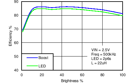
| VIN = 2.5 V | 2p6s | L = 22 µH |
| Frequency = 500 kHz | ||
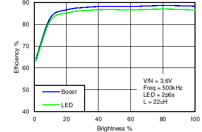
| VIN = 3.6 V | 2p6s | L = 22 µH |
| Frequency = 500 kHz | ||
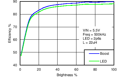
| VIN = 5.5 V | 2p6s | L = 22 µH |
| Frequency = 500 kHz | ||
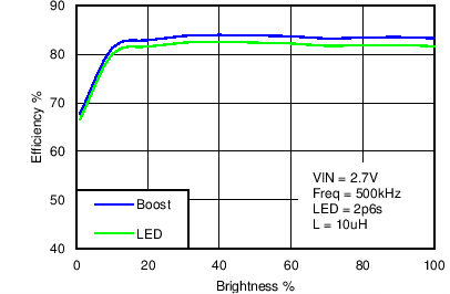
| VIN = 2.7 V | 2p6s | L = 10 µH |
| Frequency = 500 kHz | ||
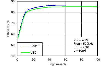
| VIN = 4.2 V | 2p6s | L = 10 µH |
| Frequency = 500 kHz | ||
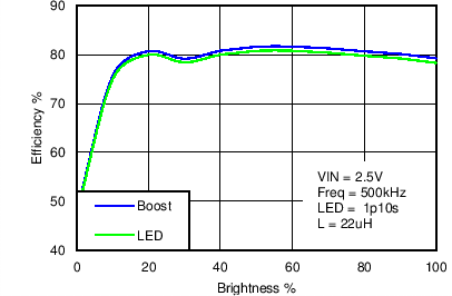
| VIN = 2.5 V | 1p10s | L = 22 µH |
| Frequency = 500 kHz | ||
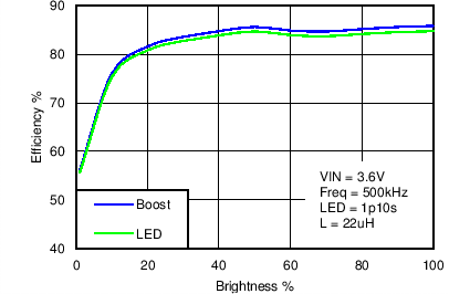
| VIN = 3.6 V | 1p10s | L = 22 µH |
| Frequency = 500 kHz | ||
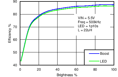
| VIN = 5.5 V | 1p10s | L = 22 µH |
| Frequency = 500 kHz | ||
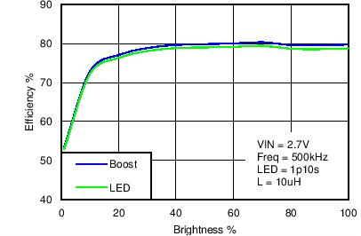
| VIN = 2.7 V | 1p10s | L = 10 µH |
| Frequency = 500 kHz | ||
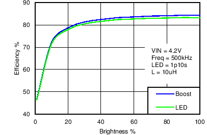
| VIN = 4.2 V | 1p10s | L = 10 µH |
| Frequency = 500 kHz | ||
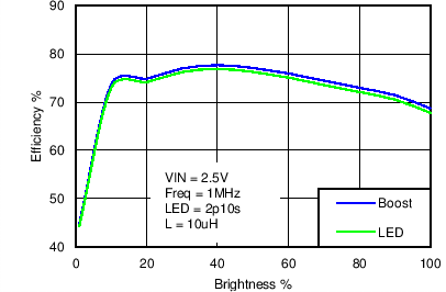
| VIN = 2.5 V | 2p10s | L = 10 µH |
| Frequency = 1 MHz | ||
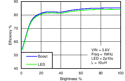
| VIN = 3.6 V | 2p10s | L = 10 µH |
| Frequency = 1 MHz |
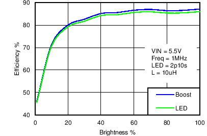
| VIN = 5.5 V | 2p10s | L = 10 µH |
| Frequency = 1 MHz | ||
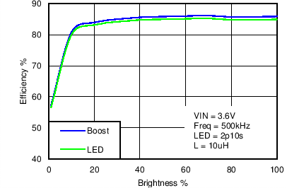
| VIN = 3.6 V | 2p10s | L = 10 µH |
| Frequency = 500 kHz | ||
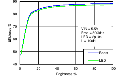
| VIN = 5.5 V | 2p10s | L = 10 µH |
| Frequency = 500 kHz | ||
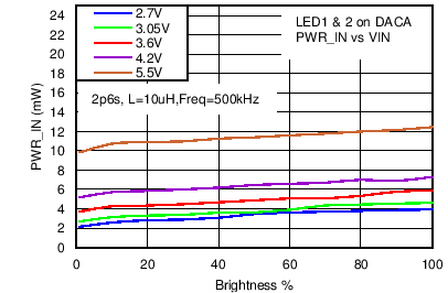
| ILED Full Scale = 28.5 mA | LED1 and 2 on DACA | |
| Frequency = 500 kHz | 2p6s | L = 10 µH |
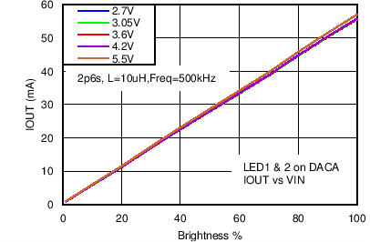
| ILED Full Scale = 28.5 mA | LED1 and 2 on DACA | |
| Frequency = 500 kHz | 2p6s | L = 10 µH |
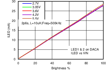
| ILED Full Scale = 28.5 mA | LED1 and 2 on DACA | |
| Frequency = 500 kHz | 2p6s | L = 10 µH |
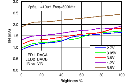
| ILED Full Scale = 28.5 mA | LED1 on DACA | 2p6s |
| Frequency = 500 kHz | LED2 on DACB | L = 10 µH |
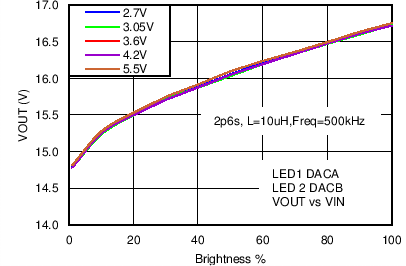
| ILED Full Scale = 28.5 mA | LED1 on DACA | 2p6s |
| Frequency = 500 kHz | LED2 on DACB | L = 10 µH |
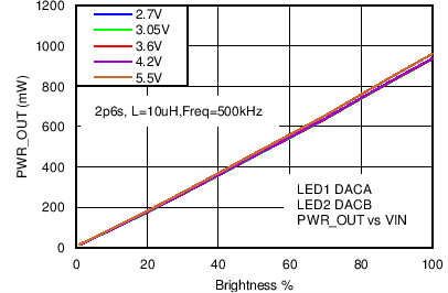
| ILED Full Scale = 28.5 mA | LED1 on DACA | 2p6s |
| Frequency = 500 kHz | LED2 on DACB | L = 10 µH |
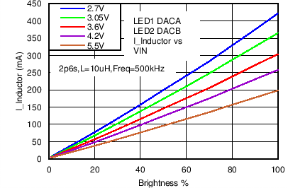
| ILED Full Scale = 28.5 mA | LED1 on DACA | 2p6s |
| Frequency = 500 kHz | LED2 on DACB | L = 10 µH |
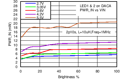
| ILED Full Scale = 28.5 mA | LED1 and LED2 on DACA | |
| Frequency = 1 MHz | 2p10s | L = 10 µH |
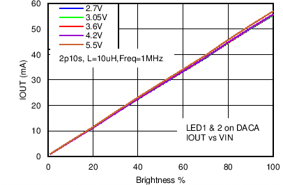
| ILED Full Scale = 28.5 mA | LED1 and LED2 on DACA | |
| Frequency = 1 MHz | 2p10s | L = 10 µH |
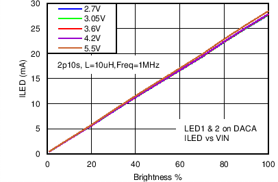
| ILED Full Scale = 28.5 mA | LED1 and LED2 on DACA | |
| Frequency = 1 MHz | 2p10s | L = 10 µH |
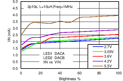
| ILED Full Scale = 28.5 mA | LED1 on DACA | 2p10s |
| Frequency = 1 MHz | LED2 on DACB | L = 10 µH |
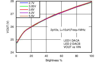
| ILED Full Scale = 28.5 mA | LED1 on DACA | 2p10s |
| Frequency = 1 MHz | LED2 on DACB | L = 10 µH |
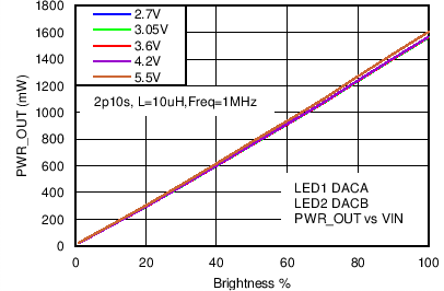
| ILED Full Scale = 28.5 mA | LED1 on DACA | 2p10s |
| Frequency = 1 MHz | LED2 on DACB | L = 10 µH |
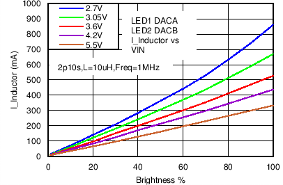
| ILED Full Scale = 28.5 mA | LED1 on DACA | 2p10s |
| Frequency = 1 MHz | LED2 on DACB | L = 10 µH |
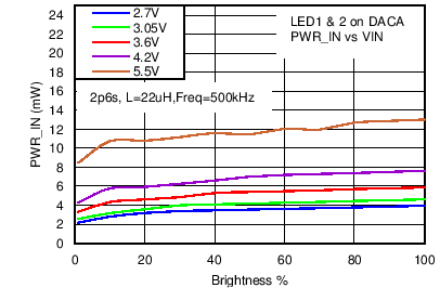
| ILED Full Scale = 28.5 mA | LED1 and LED2 on DACA | |
| Frequency = 500 kHz | 2p6s | L = 22 µH |
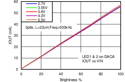
| ILED Full Scale = 28.5 mA | LED1 and LED2 on DACA | |
| Frequency = 500 kHz | 2p6s | L = 22 µH |

| ILED Full Scale = 28.5 mA | LED1 and LED2 on DACA | |
| Frequency = 500 kHz | 2p6s | L = 22 µH |
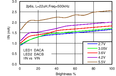
| ILED Full Scale = 28.5 mA | LED1 on DACA | 2p6s |
| Frequency = 500 kHz | LED2 on DACB | L = 22 µH |
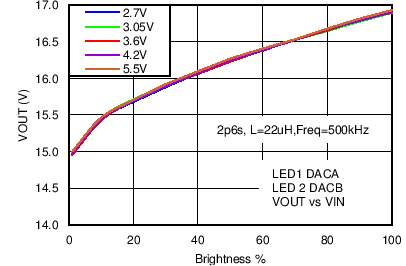
| ILED Full Scale = 28.5 mA | LED1 on DACA | 2p6s |
| Frequency = 500 kHz | LED2 on DACB | L = 22 µH |
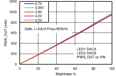
| ILED Full Scale = 28.5 mA | LED1 on DACA | 2p6s | ||
| Frequency = 500 kHz | LED2 on DACB | L = 22 µH | ||
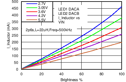
| ILED Full Scale = 28.5 mA | LED1 on DACA | 2p6s | ||
| Frequency = 500 kHz | LED2 on DACB | L = 22 µH |
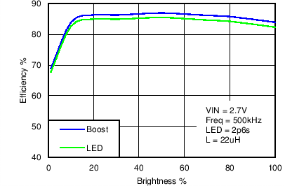
| VIN = 2.7 V | 2p6s | L = 22 µH |
| Frequency = 500 kHz | ||
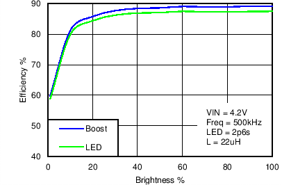
| VIN = 4.2 V | 2p6s | L = 22 µH |
| Frequency = 500 kHz | ||
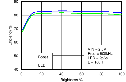
| VIN = 2.5 V | 2p6s | L = 10 µH |
| Frequency = 500 kHz | ||
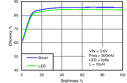
| VIN = 3.6 V | 2p6s | L = 10 µH |
| Frequency = 500 kHz | ||
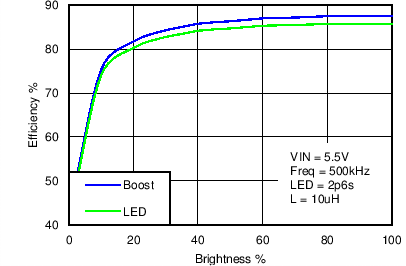
| VIN = 5.5 V | 2p6s | L = 10 µH |
| Frequency = 500 kHz | ||
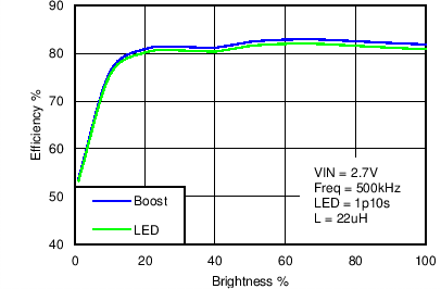
| VIN = 2.7 V | 1p10s | L = 22 µH |
| Frequency = 500 kHz | ||
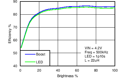
| VIN = 4.2 V | 1p10s | L = 22 µH |
| Frequency = 500 kHz | ||
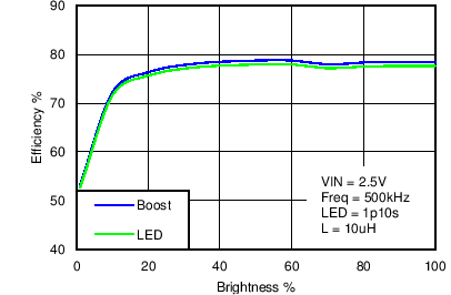
| VIN = 2.5 V | 1p10s | L = 10 µH |
| Frequency = 500 kHz | ||
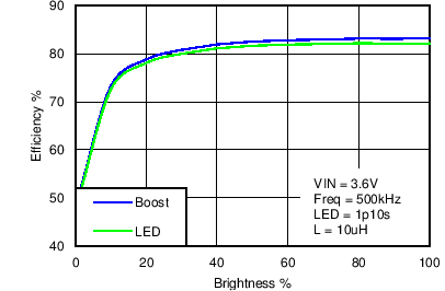
| VIN = 3.6 V | 1p10s | L = 10 µH |
| Frequency = 500 kHz | ||
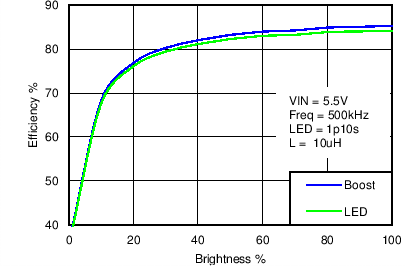
| VIN = 5.5 V | 1p10s | L = 10 µH |
| Frequency = 500 kHz | ||
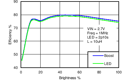
| VIN = 2.7 V | 2p10s | L = 10 µH |
| Frequency = 1 MHz | ||
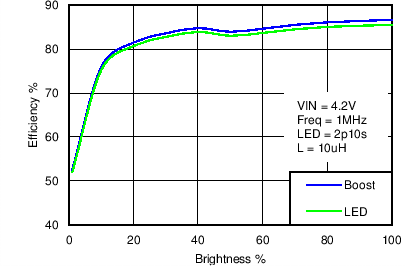
| VIN = 4.2 V | 2p10s | L = 10 µH |
| Frequency = 1 MHz | ||
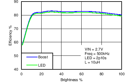
| VIN = 2.7 V | 2p10s | L = 10 µH |
| Frequency = 500 kHz | ||
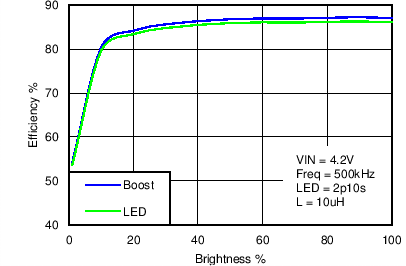
| VIN = 4.2 V | 2p10s | L = 10 µH |
| Frequency = 500 kHz | ||
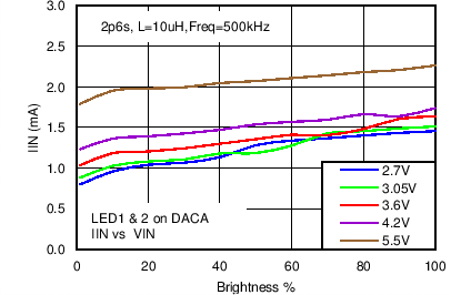
| ILED Full Scale = 28.5 mA | LED1 and 2 on DACA | |
| Frequency = 500 kHz | 2p6s | L = 10 µH |
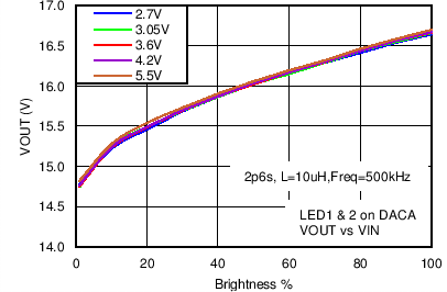
| ILED Full Scale = 28.5 mA | LED1 and 2 on DACA | |
| Frequency = 500 kHz | 2p6s | L = 10 µH |
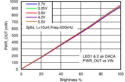
| ILED Full Scale = 28.5 mA | LED1 and 2 on DACA | |
| Frequency = 500 kHz | 2p6s | L = 10 µH |
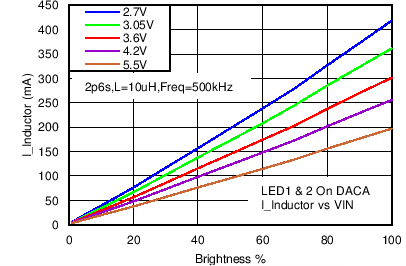
| ILED Full Scale = 28.5 mA | LED1 and 2 on DACA | |
| Frequency = 500 kHz | 2p6s | L = 10 µH |
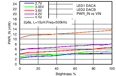
| ILED Full Scale = 28.5 mA | LED1 on DACA | 2p6s |
| Frequency = 500 kHz | LED2 on DACB | L = 10 µH |
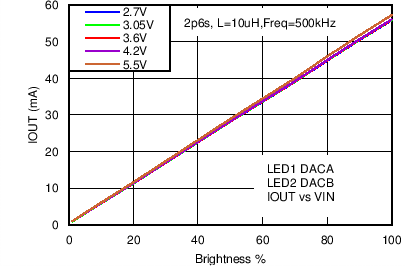
| ILED Full Scale = 28.5 mA | LED1 on DACA | 2p6s |
| Frequency = 500 kHz | LED2 on DACB | L = 10 µH |
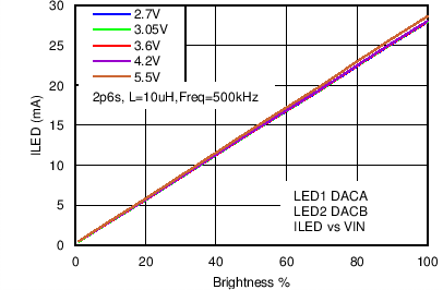
| ILED Full Scale = 28.5 mA | LED1 on DACA | 2p6s |
| Frequency = 500 kHz | LED2 on DACB | L = 10 µH |
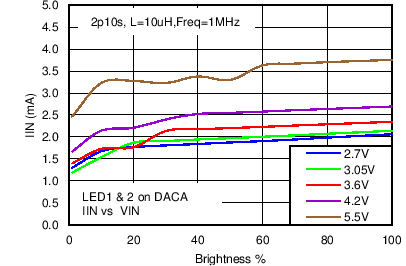
| ILED Full Scale = 28.5 mA | LED1 and LED2 on DACA | |
| Frequency = 1 MHz | 2p10s | L = 10 µH |
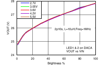
| ILED Full Scale = 28.5 mA | LED1 and LED2 on DACA | |
| Frequency = 1 MHz | 2p10s | L = 10 µH |
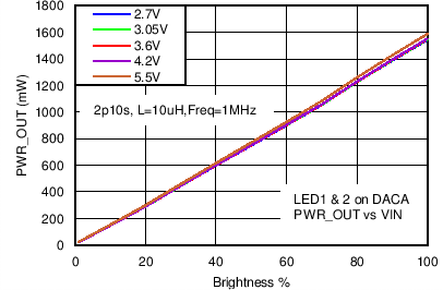
| ILED Full Scale = 28.5 mA | LED1 and LED2 on DACA | |
| Frequency = 1 MHz | 2p10s | L = 10 µH |

| ILED Full Scale = 28.5 mA | LED1 and LED2 on DACA | |
| Frequency = 1 MHz | 2p10s | L = 10 µH |
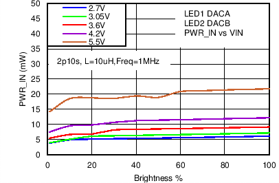
| ILED Full Scale = 28.5 mA | LED1 on DACA | 2p10s |
| Frequency = 1 MHz | LED2 on DACB | L = 10 µH |
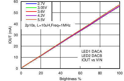
| ILED Full Scale = 28.5 mA | LED1 on DACA | 2p10s |
| Frequency = 1 MHz | LED2 on DACB | L = 10 µH |
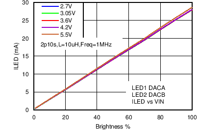
| ILED Full Scale = 28.5 mA | LED1 on DACA | 2p10s |
| Frequency = 1 MHz | LED2 on DACB | L = 10 µH |
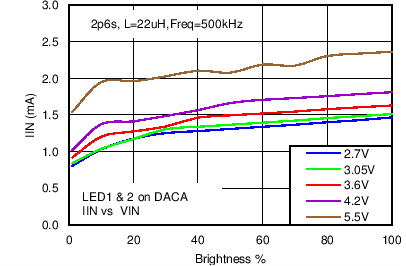
| ILED Full Scale = 28.5 mA | LED1 and LED2 on DACA | |
| Frequency = 500 kHz | 2p6s | L = 22 µH |
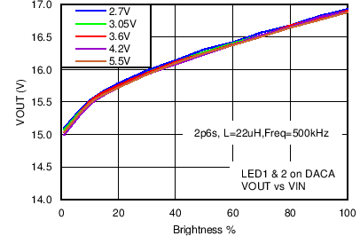
| ILED Full Scale = 28.5 mA | LED1 and LED2 on DACA | |
| Frequency = 500 kHz | 2p6s | L = 22 µH |
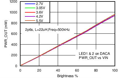
| ILED Full Scale = 28.5 mA | LED1 and LED2 on DACA | |
| Frequency = 500 kHz | 2p6s | L = 22 µH |
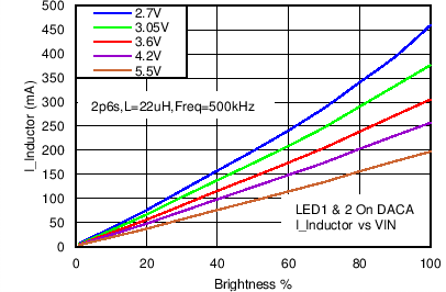
| ILED Full Scale = 28.5 mA | LED1 and LED2 on DACA | |
| Frequency = 500 kHz | 2p6s | L = 22 µH |
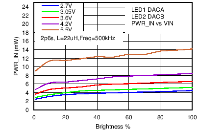
| ILED Full Scale = 28.5 mA | LED1 on DACA | 2p6s |
| Frequency = 500 kHz | LED2 on DACB | L = 22 µH |
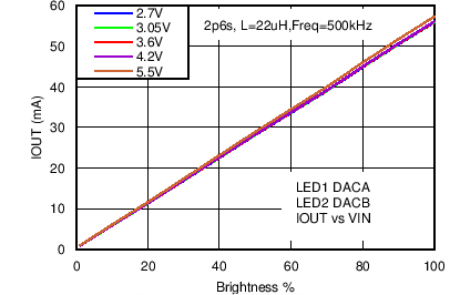
| ILED Full Scale = 28.5 mA | LED1 on DACA | 2p6s |
| Frequency = 500 kHz | LED2 on DACB | L = 22 µH |

| ILED Full Scale = 28.5 mA | LED1 on DACA | 2p6s |
| Frequency = 500 kHz | LED2 on DACB | L = 22 µH |