SNVS555D January 2008 – December 2014 LM3881
PRODUCTION DATA.
- 1 Features
- 2 Applications
- 3 Description
- 4 Revision History
- 5 Pin Configuration and Functions
- 6 Specifications
- 7 Detailed Description
- 8 Application and Implementation
- 9 Power Supply Recommendations
- 10Layout
- 11Device and Documentation Support
- 12Mechanical, Packaging, and Orderable Information
パッケージ・オプション
メカニカル・データ(パッケージ|ピン)
- DGK|8
サーマルパッド・メカニカル・データ
- DGK|8
発注情報
1 Features
- Easiest Method to Sequence Rails
- Power-Up and Power-Down Control
- Tiny Footprint
- Low Quiescent Current of 80 µA
- Input Voltage Range of 2.7 V to 5.5 V
- Output Invert Feature
- Timing Controlled by Small Value External Capacitor
2 Applications
- Security Cameras
- Servers
- Networking Elements
- FPGA Sequencing
- Microprocessor and Microcontroller Sequencing
- Multiple Supply Sequencing
3 Description
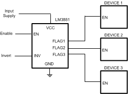
The LM3881 Simple Power Sequencer offers the easiest method to control power up and power down of multiple power supplies (switching or linear regulators). By staggering the start-up sequence, it is possible to avoid latch conditions or large inrush currents that can affect the reliability of the system.
Available in VSSOP-8 package, the Simple Sequencer contains a precision enable pin and three open-drain output flags. When the LM3881 is enabled, the three output flags will sequentially release, after individual time delays, thus permitting the connected power supplies to start up. The output flags will follow a reverse sequence during power down to avoid latch conditions. Time delays are defined using an external capacitor and the output flag states can be inverted by the user.
Device Information(1)
| PART NUMBER | PACKAGE | BODY SIZE (NOM) |
|---|---|---|
| LM3881 | VSSOP (8) | 3.00 mm x 3.00 mm |
- For all available packages, see the orderable addendum at the end of the datasheet.
Typical System Application