SNVS628H October 2009 – December 2019 LM5060
PRODUCTION DATA.
- 1 Features
- 2 Applications
- 3 Description
- 4 Revision History
- 5 Pin Configuration and Functions
- 6 Specifications
- 7 Detailed Description
-
8 Application and Implementation
- 8.1 Application Information
- 8.2
Typical Applications
- 8.2.1
Example Number 1: LM5060EVAL Design
- 8.2.1.1 Design Requirements
- 8.2.1.2
Detailed Design Procedure
- 8.2.1.2.1 VDS Fault Detection and Selecting Sense Pin Resistor RS
- 8.2.1.2.2 Turn-On Time
- 8.2.1.2.3 Fault Detection Delay Time
- 8.2.1.2.4 MOSFET Selection
- 8.2.1.2.5 Input and Output Capacitors
- 8.2.1.2.6 UVLO, OVP
- 8.2.1.2.7 POWER GOOD Indicator
- 8.2.1.2.8 Input Bypass Capacitor
- 8.2.1.2.9 Large Load Capacitance
- 8.2.1.3 Application Curves
- 8.2.2 Example Number 2: Reverse Polarity Protection With Diodes
- 8.2.3 Example Number 3: Reverse Polarity Protection With Resistor
- 8.2.1
Example Number 1: LM5060EVAL Design
- 9 Power Supply Recommendations
- 10Layout
- 11Device and Documentation Support
- 12Mechanical, Packaging, and Orderable Information
7.4.1 Power-Up Sequence
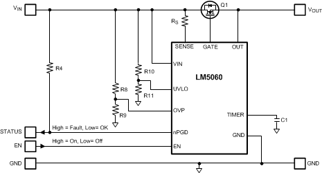
The basic application circuit is shown in Figure 20 and a normal start-up sequence is shown in Figure 21. Start-up of the LM5060 is initiated when the EN pin is above the (ENTHH) threshold (2.0 V). At start-up, the timer capacitor is charged with a 6-µA (typical) current source while the gate of the external N-channel MOSFET is charged through the GATE pin by a 24-µA (typical) current source.
When the gate-to-source voltage (VGS) reaches the VGATE-TH threshold (typically 5 V) the VGS sequence ends, the timer capacitor is quickly discharged to 0.3 V, and the 5-µA current source is enabled.
The timer capacitor will charge until either the VDS Comparator indicates that the drain-to-source voltage (VDS) has been reduced to a nominal value (i.e. no fault) or the voltage on the timer capacitor has reached the VTMRH threshold (i.e. fault). The VDS Comparator monitors the voltage difference between the SENSE pin and the OUT pin. The SENSE pin voltage is user programmed to be lower than the input supply voltage by selecting a suitable sense resistor value. When the OUT pin voltage exceeds the voltage at the SENSE pin, the nPGD pin is asserted low (i.e. no fault) and the timer capacitor is discharged.
 Figure 20. Basic Application Circuit