SNVS628H October 2009 – December 2019 LM5060
PRODUCTION DATA.
- 1 Features
- 2 Applications
- 3 Description
- 4 Revision History
- 5 Pin Configuration and Functions
- 6 Specifications
- 7 Detailed Description
-
8 Application and Implementation
- 8.1 Application Information
- 8.2
Typical Applications
- 8.2.1
Example Number 1: LM5060EVAL Design
- 8.2.1.1 Design Requirements
- 8.2.1.2
Detailed Design Procedure
- 8.2.1.2.1 VDS Fault Detection and Selecting Sense Pin Resistor RS
- 8.2.1.2.2 Turn-On Time
- 8.2.1.2.3 Fault Detection Delay Time
- 8.2.1.2.4 MOSFET Selection
- 8.2.1.2.5 Input and Output Capacitors
- 8.2.1.2.6 UVLO, OVP
- 8.2.1.2.7 POWER GOOD Indicator
- 8.2.1.2.8 Input Bypass Capacitor
- 8.2.1.2.9 Large Load Capacitance
- 8.2.1.3 Application Curves
- 8.2.2 Example Number 2: Reverse Polarity Protection With Diodes
- 8.2.3 Example Number 3: Reverse Polarity Protection With Resistor
- 8.2.1
Example Number 1: LM5060EVAL Design
- 9 Power Supply Recommendations
- 10Layout
- 11Device and Documentation Support
- 12Mechanical, Packaging, and Orderable Information
8.2.1.2.2 Turn-On Time
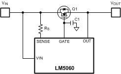
To slow down the output rise time a capacitor from the GATE pin to GND may be added. The turn on time depends on the threshold level of the N-Channel MOSFET, the gate capacitance of the MOSFET as well as the optional capacitance from the GATE pin to GND. Figure 28 shows the slow down capacitor C1. Reducing the turn-on time allows the MOSFET (Q1), to slowly charge a large load capacitance. Special care must be taken to keep the MOSFET within its safe operating area. If the MOSFET turns on too slow, the peak power losses may damage the device.
 Figure 28. Turn-On Time Extension