SNVS628H October 2009 – December 2019 LM5060
PRODUCTION DATA.
- 1 Features
- 2 Applications
- 3 Description
- 4 Revision History
- 5 Pin Configuration and Functions
- 6 Specifications
- 7 Detailed Description
-
8 Application and Implementation
- 8.1 Application Information
- 8.2
Typical Applications
- 8.2.1
Example Number 1: LM5060EVAL Design
- 8.2.1.1 Design Requirements
- 8.2.1.2
Detailed Design Procedure
- 8.2.1.2.1 VDS Fault Detection and Selecting Sense Pin Resistor RS
- 8.2.1.2.2 Turn-On Time
- 8.2.1.2.3 Fault Detection Delay Time
- 8.2.1.2.4 MOSFET Selection
- 8.2.1.2.5 Input and Output Capacitors
- 8.2.1.2.6 UVLO, OVP
- 8.2.1.2.7 POWER GOOD Indicator
- 8.2.1.2.8 Input Bypass Capacitor
- 8.2.1.2.9 Large Load Capacitance
- 8.2.1.3 Application Curves
- 8.2.2 Example Number 2: Reverse Polarity Protection With Diodes
- 8.2.3 Example Number 3: Reverse Polarity Protection With Resistor
- 8.2.1
Example Number 1: LM5060EVAL Design
- 9 Power Supply Recommendations
- 10Layout
- 11Device and Documentation Support
- 12Mechanical, Packaging, and Orderable Information
8.1.8 UVLO
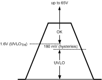
The UVLO function will turn off the external N-Channel MOSFET with a 2.2 mA (typical) current sink at the GATE pin. Figure 25 shows the threshold levels of the UVLO input. A resistor divider as shown in Figure 20 with R10 and R11 sets the voltage at which the UVLO function engages. The UVLO pin may also be used as a second enable pin for applications requiring a redundant, or secondary, shut-down control. Unlike the EN pin function, the UVLO function does not switch the LM5060 to the low current (disabled) state.
If the UVLO function is not needed, the UVLO pin should be connected to the VIN pin. The UVLO pin should not be left floating as the internal pull-down will keep the UVLO active.
In addition to the programmable UVLO function, an internal Power-On-Reset (POR) monitors the voltage at the VIN pin and turns the MOSFET Off when VIN falls below typically 5.10 V.
 Figure 25. UVLO Threshold Levels