SNVS628H October 2009 – December 2019 LM5060
PRODUCTION DATA.
- 1 Features
- 2 Applications
- 3 Description
- 4 Revision History
- 5 Pin Configuration and Functions
- 6 Specifications
- 7 Detailed Description
-
8 Application and Implementation
- 8.1 Application Information
- 8.2
Typical Applications
- 8.2.1
Example Number 1: LM5060EVAL Design
- 8.2.1.1 Design Requirements
- 8.2.1.2
Detailed Design Procedure
- 8.2.1.2.1 VDS Fault Detection and Selecting Sense Pin Resistor RS
- 8.2.1.2.2 Turn-On Time
- 8.2.1.2.3 Fault Detection Delay Time
- 8.2.1.2.4 MOSFET Selection
- 8.2.1.2.5 Input and Output Capacitors
- 8.2.1.2.6 UVLO, OVP
- 8.2.1.2.7 POWER GOOD Indicator
- 8.2.1.2.8 Input Bypass Capacitor
- 8.2.1.2.9 Large Load Capacitance
- 8.2.1.3 Application Curves
- 8.2.2 Example Number 2: Reverse Polarity Protection With Diodes
- 8.2.3 Example Number 3: Reverse Polarity Protection With Resistor
- 8.2.1
Example Number 1: LM5060EVAL Design
- 9 Power Supply Recommendations
- 10Layout
- 11Device and Documentation Support
- 12Mechanical, Packaging, and Orderable Information
8.1.3 VGS Considerations
The VGS Status Comparator accomplishes two purposes:
- As the gate of the external MOSFET is charged, the VGS voltage transitions from cut-off, through an active region, and into the ohmic region. The LM5060 provides two fault timer modes to monitor these transitions. The TIMER pin capacitor is initially charged with a constant 6 µA (typical) until either the MOSFET VGS reaches the VGATE–TH threshold (typically 5 V) indicating that the MOSFET channel is at least somewhat enhanced, or the voltage on the TIMER pin reaches the VTMRH threshold (typically 2 V) indicating a fault condition. If the MOSFET VGS reaches 5-V threshold before the TIMER pin reaches the typical 2 V timer fault threshold, the timer capacitor is then discharged to 300 mV, and then begins charging with 11-µA current source while the MOSFET transitions through the active region. The lower timer capacitor charge current during the initial start-up sequence allows more time before a fault is indicated. The turn-on time of the MOSFET will vary with input voltage, load capacitance, load resistance, as well as the MOSFET characteristics.
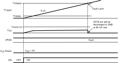
- Figure 22 shows a start-up waveform with excessive gate leakage. The initial charge current on the timer capacitor is 6 µA (typical), while the simultaneous charge current to the gate is 24 µA (typical). Due to excessive gate leakage, the 24 µA is not able to charge the gate to the required typical 5 V VGS threshold and the VDS Fault Comparator will indicate a fault when the timer capacitor is charged to the VTMRH fault threshold. When the timer capacitor voltage reaches theVTMRH fault threshold (typically 2 V) the MOSFET gate is discharged at an 80 mA (typical) rate.
 Figure 22. Voltages During Startup With VGS Gate Leakage Condition