JAJSFG5D November 2008 – May 2018 LM7705
PRODUCTION DATA.
- 1 特長
- 2 アプリケーション
- 3 概要
- 4 改訂履歴
- 5 Pin Configuration and Functions
- 6 Specifications
- 7 Detailed Description
- 8 Application and Implementation
- 9 Power Supply Recommendations
- 10Layout
- 11デバイスおよびドキュメントのサポート
- 12メカニカル、パッケージ、および注文情報
パッケージ・オプション
メカニカル・データ(パッケージ|ピン)
- DGK|8
サーマルパッド・メカニカル・データ
- DGK|8
発注情報
7.4.1.3 Dual-Supply, True Zero Amplifiers
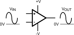
The limitations of the output stage of the op amp, as indicated in both examples, can be omitted by using a dual supply op amp. The output stage of the used op amp can then still swing from 50 mV of the supply rails. However, the functional output range of the op amp is now from ground level to a value near the positive supply rail. Figure 26 shows the output drive of an amplifier in a true zero output voltage application.
 Figure 26. Amplifier Output Drive With a Dual-Supply
 Disadvantages of this solution are:
- The usage of a dual-supply instead of a simple single supply is more expensive.
- A dual supply voltage for the op amps requires parts that can handle a larger operating range for the supply voltage. If the op amps used in the current solution cannot handle this, a redesign can be required.
A better solution is to use the LM7705. This low-noise negative bias generator has some major advantages with respect to a dual-supply solution:
- Operates with only a single positive supply, and is therefore a much cheaper solution.
- The LM7705 generates a negative supply voltage of only −0.23 V. This is more than enough to create a True-zero output for most op amps.
- In many applications, this small extension of the supply voltage range can be within the abs max rating for many op amps, so an expensive redesign is not necessary.
In the Typical Application section, a typical amplifier application will be evaluated. The performance of an amplifier will be measured in a single supply configuration. The results will be compared with an amplifier using a LM7705 supplying a negative voltage to the bias pin.