JAJSFG5D November 2008 – May 2018 LM7705
PRODUCTION DATA.
- 1 特長
- 2 アプリケーション
- 3 概要
- 4 改訂履歴
- 5 Pin Configuration and Functions
- 6 Specifications
- 7 Detailed Description
- 8 Application and Implementation
- 9 Power Supply Recommendations
- 10Layout
- 11デバイスおよびドキュメントのサポート
- 12メカニカル、パッケージ、および注文情報
パッケージ・オプション
メカニカル・データ(パッケージ|ピン)
- DGK|8
サーマルパッド・メカニカル・データ
- DGK|8
発注情報
8.1.1 Functional Description
The LM7705, low-noise negative bias generator, can be used for many applications requiring a fixed negative voltage. A key application for the LM7705 is an amplifier with a true zero output voltage using the original parts, while not exceeding the maximum supply voltage ratings of the amplifier.
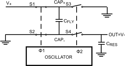
The voltage inversion in the LM7705 is achieved using a switched capacitor technique with two external capacitors (CFLY and CRES). An internal oscillator and a switching network transfers charge between the two storage capacitors. This switched capacitor technique is given in Figure 27.
 Figure 27. Voltage Inverter
 The internal oscillator generates two anti-phase clock signals. Clock 1 controls switches S1 and S2. Clock 2 controls switches S3 and S4. When Switches S1 and S2 are closed, capacitor CFLY is charged to V+. When switches S3 and S4 are closed (S1 and S2 are open) charge from CFLY is transferred to CRES and the output voltage OUT is equal to –V+.
Due to the switched capacitor technique, a small ripple will be present at the output voltage with a frequency of the oscillator. The magnitude of this ripple will increase for increasing output currents. The magnitude of the ripple can be influenced by changing the values of the used capacitors.