JAJSFG5D November 2008 – May 2018 LM7705
PRODUCTION DATA.
- 1 特長
- 2 アプリケーション
- 3 概要
- 4 改訂履歴
- 5 Pin Configuration and Functions
- 6 Specifications
- 7 Detailed Description
- 8 Application and Implementation
- 9 Power Supply Recommendations
- 10Layout
- 11デバイスおよびドキュメントのサポート
- 12メカニカル、パッケージ、および注文情報
パッケージ・オプション
メカニカル・データ(パッケージ|ピン)
- DGK|8
サーマルパッド・メカニカル・データ
- DGK|8
発注情報
8.1.2 Technical Description
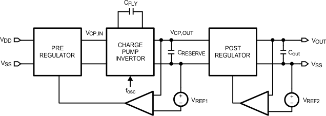
As indicated in Functional Description, the main function of the LM7705 is to supply a stabilized negative bias voltage to a load, using only a positive supply voltage. A general block diagram for this charge pump inverter is given in Figure 28. The external power supply and load are added in this diagram as well.
 Figure 28. LM7705 Architecture
 The architecture given in Figure 28 shows that the LM7705 contains 3 functional blocks:
- Pre-regulator
- Charge pump inverter
- Post-regulator
The output voltage is stabilized by:
- Controlling the power supplied from the power supply to the charge pump input by the pre-regulator
- The power supplied from the charge pump output to the load by the post-regulator.
A more detailed block diagram of the negative bias generator is given in Figure 29. The control of the pre-regulator is based on measuring the output voltage of the charge pump. The goal of the post-regulator is to provide an accurate controlled negative voltage at the output, and acts as a lowpass filter to attenuate the output voltage ripple. The voltage ripple is a result of the switching behavior of the charge pump and is dependent of the output current and the values of the used capacitors.
 Figure 29. Charge Pump Inverter With Input and Output Control
 In Charge Pump Theory, a simple equation will be derived that shows the relation between the ripple of the output current, the frequency of the internal clock generator and the value of the capacitor placed at the output of the LM7705.