JAJSEU5D October   2014  – February 2018 LMH5401

PRODUCTION DATA.  

  1. 特長
  2. アプリケーション
    1.     歪みと周波数との関係(G=12dB、SE-DE、RL=200rep%#937;、VPP=2V)
  3. 概要
    1.     ADC12J4000を駆動するLMH5401
  4. 改訂履歴
  5. Pin Configuration and Functions
    1.     Pin Functions
  6. Specifications
    1. 6.1 Absolute Maximum Ratings
    2. 6.2 ESD Ratings
    3. 6.3 Recommended Operating Conditions
    4. 6.4 Thermal Information
    5. 6.5 Electrical Characteristics: VS = 5 V
    6. 6.6 Electrical Characteristics: VS = 3.3 V
    7. 6.7 Typical Characteristics: 5 V
    8. 6.8 Typical Characteristics: 3.3 V
    9. 6.9 Typical Characteristics: 3.3-V to 5-V Supply Range
  7. Parameter Measurement Information
    1. 7.1  Output Reference Points
    2. 7.2  ATE Testing and DC Measurements
    3. 7.3  Frequency Response
    4. 7.4  S-Parameters
    5. 7.5  Frequency Response with Capacitive Load
    6. 7.6  Distortion
    7. 7.7  Noise Figure
    8. 7.8  Pulse Response, Slew Rate, and Overdrive Recovery
    9. 7.9  Power Down
    10. 7.10 VCM Frequency Response
    11. 7.11 Test Schematics
  8. Detailed Description
    1. 8.1 Overview
    2. 8.2 Functional Block Diagram
    3. 8.3 Feature Description
      1. 8.3.1 Fully-Differential Amplifier
        1. 8.3.1.1 Power Down and Ground Pins
      2. 8.3.2 Operations for Single-Ended to Differential Signals
        1. 8.3.2.1 AC-Coupled Signal Path Considerations for Single-Ended Input to Differential Output Conversion
        2. 8.3.2.2 DC-Coupled Input Signal Path Considerations for SE-DE Conversions
        3. 8.3.2.3 Resistor Design Equations for Single-to-Differential Applications
        4. 8.3.2.4 Input Impedance Calculations
      3. 8.3.3 Differential-to-Differential Signals
        1. 8.3.3.1 AC-Coupled, Differential-Input to Differential-Output Design Issues
        2. 8.3.3.2 DC-Coupled, Differential-Input to Differential-Output Design Issues
      4. 8.3.4 Output Common-Mode Voltage
      5. 8.3.5 LMH5401 Comparison
    4. 8.4 Device Functional Modes
      1. 8.4.1 Operation With a Split Supply
      2. 8.4.2 Operation With a Single Supply
  9. Application and Implementation
    1. 9.1 Application Information
      1. 9.1.1 Stability
      2. 9.1.2 Input and Output Headroom Considerations
      3. 9.1.3 Noise Analysis
      4. 9.1.4 Noise Figure
      5. 9.1.5 Thermal Considerations
    2. 9.2 Typical Application
      1. 9.2.1 Design Requirements
      2. 9.2.2 Detailed Design Procedure
        1. 9.2.2.1 Driving Matched Loads
        2. 9.2.2.2 Driving Unmatched Loads For Lower Loss
        3. 9.2.2.3 Driving Capacitive Loads
        4. 9.2.2.4 Driving ADCs
          1. 9.2.2.4.1 SNR Considerations
          2. 9.2.2.4.2 SFDR Considerations
          3. 9.2.2.4.3 ADC Input Common-Mode Voltage Considerations : AC-Coupled Input
          4. 9.2.2.4.4 ADC Input Common-Mode Voltage Considerations : DC-Coupled Input
        5. 9.2.2.5 GSPS ADC Driver
        6. 9.2.2.6 Common-Mode Voltage Correction
        7. 9.2.2.7 Active Balun
      3. 9.2.3 Application Curves
    3. 9.3 Do's and Don'ts
      1. 9.3.1 Do:
      2. 9.3.2 Don't:
  10. 10Power Supply Recommendations
    1. 10.1 Supply Voltage
    2. 10.2 Single-Supply
    3. 10.3 Split-Supply
    4. 10.4 Supply Decoupling
  11. 11Layout
    1. 11.1 Layout Guidelines
    2. 11.2 Layout Example
  12. 12デバイスおよびドキュメントのサポート
    1. 12.1 デバイス・サポート
      1. 12.1.1 デバイスの項目表記
    2. 12.2 ドキュメントのサポート
      1. 12.2.1 関連資料
    3. 12.3 ドキュメントの更新通知を受け取る方法
    4. 12.4 コミュニティ・リソース
    5. 12.5 商標
    6. 12.6 静電気放電に関する注意事項
    7. 12.7 Glossary
  13. 13メカニカル、パッケージ、および注文情報

パッケージ・オプション

メカニカル・データ(パッケージ|ピン)
サーマルパッド・メカニカル・データ
発注情報

Typical Characteristics: 5 V

at TA = 25°C, split supplies, VCM = 0 V, RL = 200-Ω differential (RO = 40 Ω each), G = 12 dB (4 V/V), single-ended input and differential output, and input and output pins referenced to midsupply, (unless otherwise noted.) Measured using an EVM as discussed in the section (see Figure 56 to Figure 59).
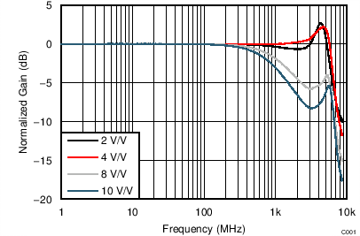
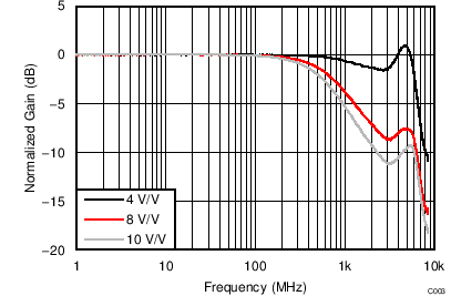
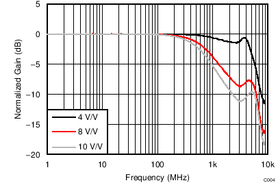
LMH5401 TC_C001_Freq_Gain_5V_0p2Vpp.png
VS = ±2.5 V, VOUT_AMP = 0.2 VPP, RL = 200 Ω
Figure 1. Small-Signal Frequency Response vs Gain
LMH5401 TC_C003_Freq_RLd_5V_0p2Vpp_diff.png
VOUT_AMP = 0.2 VPP, RL = 200 Ω
Figure 3. Differential Input Small-Signal Frequency Response vs Gain
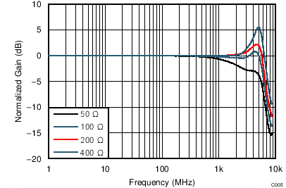
LMH5401 TC_C005_Freq_RLoad_5V_0p2Vpp.png
VS = ±2.5 V, VOUT_AMP = 2 VPP, G = 12 dB, SE-DE
Figure 5. Small-Signal Frequency Response vs Load
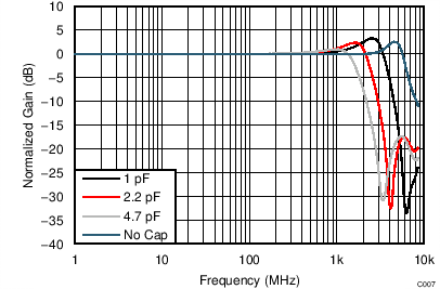
LMH5401 TC_C007_Freq_CLoad_5V_0p2Vpp.png
VS = ±2.5 V, VOUT_AMP = 0.2 VPP, capacitance at DUT output pins, G = 12 dB, SE-DE
Figure 7. Small-Signal Frequency Response vs Capacitive Load
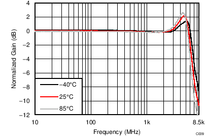
LMH5401 TC_C009_Freq_Temp_5V.png
VS = ±2.5 V, VOUT_AMP = 2 VPP, G = 12 dB, SE-DE
Figure 9. Bandwidth vs Temperature
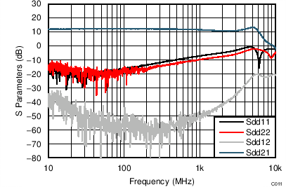
LMH5401 TC_C011_Sparam_5V_Diff.png
VS = ±2.5 V, VOUT_AMP = 200 mVPP
Figure 11. S-Parameters Differential Input (±2.5-V Supply)
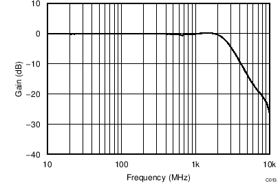
LMH5401 TC_C013_Freq_CM_0p2Vpp_5V.png
VS = ±2.5 V, VOUT_AMP = 200 mVPP
Figure 13. Common-Mode Frequency Response
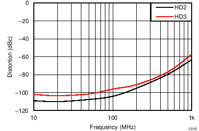
LMH5401 TC_C015_H23_5V_Freq_DIffIn.png
VS = ±2.5 V, VOUT_AMP = 2 VPP
(Differential to Differential, RL = 200 Ω)
Figure 15. HD2 and HD3 vs Frequency
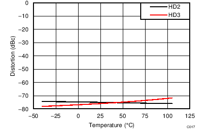
LMH5401 TC_C017_HD23_Temp_5V.png
VS = ±2.5 V, VOUT_AMP = 2 VPP, RL = 200 Ω, f = 500 MHz
Figure 17. HD2 and HD3 vs Temperature
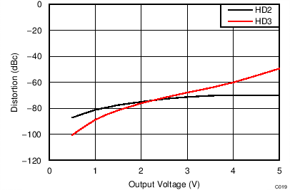
LMH5401 TC_C019_H23_5V_Vout.png
VS = ±2.5 V, f = 500 MHz
Figure 19. HD2 and HD3 vs Output Voltage
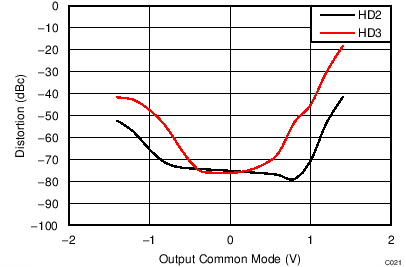
LMH5401 TC_C021_H23_5V_Vocm.png
VS = ±2.5 V, f = 500 MHz , VOUT_AMP = 2 VPP
Figure 21. HD2 and HD3 vs Output Common-Mode Voltage
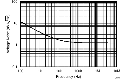
LMH5401 TC_C023_voltage_noise_sbos710.png
VS = ±2.5 V
Figure 23. Input-Referred Voltage Noise
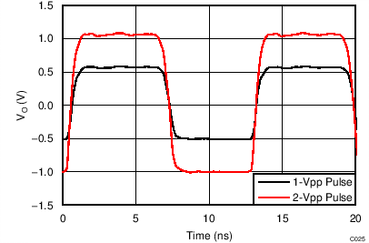
LMH5401 TC_C025_Pulse_5V_Diff.png
VS = ±2.5 V, VOUT_AMP
Figure 25. Pulse Response for Various VO
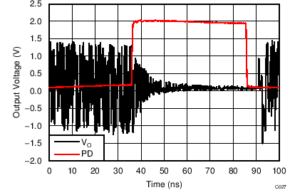
LMH5401 TC_C027_PDTime_5V_bos695.png
VS = ±2.5 V
Figure 27. Power-Down Timing
LMH5401 TC_C002_Freq_Gain_5V_2Vpp.png
VOUT_AMP = 2 VPP, RL = 200 Ω
Figure 2. Large-Signal Frequency Response vs Gain
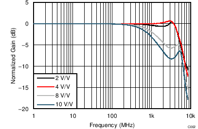
LMH5401 TC_C004_Freq_RLoad_5V_2Vpp_diff.png
VOUT_AMP = 2 VPP, RL = 200 Ω
Figure 4. Differential Input Large-Signal Frequency Response vs Gain
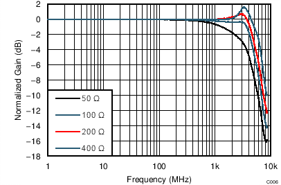
LMH5401 TC_C006_Freq_RLoad_5V_2Vpp.png
VS = ±2.5 V, VOUT_AMP = 2 VPP, G = 12 dB, SE-DE
Figure 6. Large-Signal Frequency Response vs Load
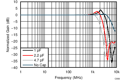
LMH5401 TC_C008_Freq_CLoad_5V_2Vpp.png
VS = ±2.5 V, VOUT_AMP = 2 VPP, capacitance at DUT output pins, G = 12 dB, SE-DE
Figure 8. Large-Signal Frequency Response vs Capacitive Load
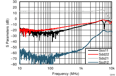
LMH5401 TC_C010_Sparam_SEin_5V.png
VS = ±2.5 V, VOUT_AMP = 200 mVPP, ±2.5-V supply
Figure 10. S-Parameters Single-Ended Input
LMH5401 TC_C012_Balance_Error_5V.png
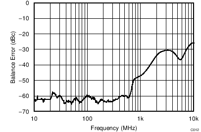
VS = ±2.5 V, VOUT_AMP = 200 mVPP
Figure 12. Balance Error
LMH5401 TC_C014_H23_5V_Freq_SEIn.png
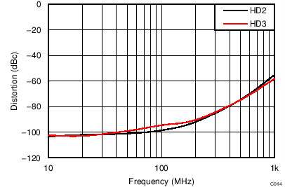
VS = ±2.5 V, VOUT_AMP = 2 VPP, SE-DE, RL = 200 Ω
Figure 14. HD2 and HD3 vs Frequency
LMH5401 TC_C016_H23_5V_Freq_SEIn_RL100.png
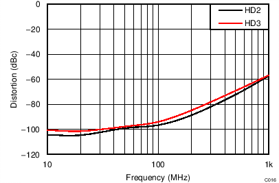
VS = ±2.5 V, VOUT_AMP = 2 VPP, (SE-DE, RL = 100 Ω)
Figure 16. HD2 and HD3 vs Frequency
LMH5401 TC_C018_H23_5V_RLoad.png
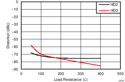
VS = ±2.5 V, VOUT_AMP = 2 VPP, f = 500 MHz
Figure 18. HD2 and HD3 vs Load Resistance
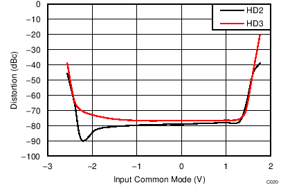
LMH5401 TC_C020_H23_5V_Vicm.png
VS = ±2.5 V, VOUT_AMP = 2 VPP, f = 500 MHz
Figure 20. HD2 and HD3 vs Input Common-Mode Voltage
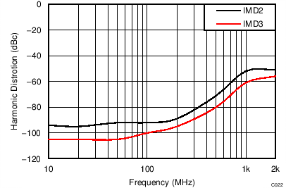
LMH5401 TC_C022_IMD23_Frequency_5V.png
VS = ±2.5 V, VOUT_AMP = 1 VPP per tone
Figure 22. Intermodulation vs Frequency
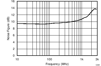
LMH5401 TC_C024_NoiseFig_Freq_5V.png
VS = ±2.5 V
Figure 24. Noise Figure vs Frequency
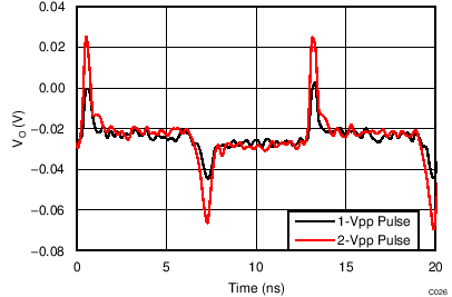
LMH5401 TC_C026_Pulse_5V_CM.png
VS = ±2.5 V, VOUT_AMP, VCM = (VO+ + VO–) / 2
Figure 26. Pulse Response Common-Mode for Various VO
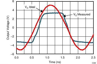
LMH5401 TC_C028_Overdrive_5v_bos695.png
VS = ±2.5 V
Figure 28. Overdrive Recovery