JAJSEU5D October   2014  – February 2018 LMH5401

PRODUCTION DATA.  

  1. 特長
  2. アプリケーション
    1.     歪みと周波数との関係(G=12dB、SE-DE、RL=200rep%#937;、VPP=2V)
  3. 概要
    1.     ADC12J4000を駆動するLMH5401
  4. 改訂履歴
  5. Pin Configuration and Functions
    1.     Pin Functions
  6. Specifications
    1. 6.1 Absolute Maximum Ratings
    2. 6.2 ESD Ratings
    3. 6.3 Recommended Operating Conditions
    4. 6.4 Thermal Information
    5. 6.5 Electrical Characteristics: VS = 5 V
    6. 6.6 Electrical Characteristics: VS = 3.3 V
    7. 6.7 Typical Characteristics: 5 V
    8. 6.8 Typical Characteristics: 3.3 V
    9. 6.9 Typical Characteristics: 3.3-V to 5-V Supply Range
  7. Parameter Measurement Information
    1. 7.1  Output Reference Points
    2. 7.2  ATE Testing and DC Measurements
    3. 7.3  Frequency Response
    4. 7.4  S-Parameters
    5. 7.5  Frequency Response with Capacitive Load
    6. 7.6  Distortion
    7. 7.7  Noise Figure
    8. 7.8  Pulse Response, Slew Rate, and Overdrive Recovery
    9. 7.9  Power Down
    10. 7.10 VCM Frequency Response
    11. 7.11 Test Schematics
  8. Detailed Description
    1. 8.1 Overview
    2. 8.2 Functional Block Diagram
    3. 8.3 Feature Description
      1. 8.3.1 Fully-Differential Amplifier
        1. 8.3.1.1 Power Down and Ground Pins
      2. 8.3.2 Operations for Single-Ended to Differential Signals
        1. 8.3.2.1 AC-Coupled Signal Path Considerations for Single-Ended Input to Differential Output Conversion
        2. 8.3.2.2 DC-Coupled Input Signal Path Considerations for SE-DE Conversions
        3. 8.3.2.3 Resistor Design Equations for Single-to-Differential Applications
        4. 8.3.2.4 Input Impedance Calculations
      3. 8.3.3 Differential-to-Differential Signals
        1. 8.3.3.1 AC-Coupled, Differential-Input to Differential-Output Design Issues
        2. 8.3.3.2 DC-Coupled, Differential-Input to Differential-Output Design Issues
      4. 8.3.4 Output Common-Mode Voltage
      5. 8.3.5 LMH5401 Comparison
    4. 8.4 Device Functional Modes
      1. 8.4.1 Operation With a Split Supply
      2. 8.4.2 Operation With a Single Supply
  9. Application and Implementation
    1. 9.1 Application Information
      1. 9.1.1 Stability
      2. 9.1.2 Input and Output Headroom Considerations
      3. 9.1.3 Noise Analysis
      4. 9.1.4 Noise Figure
      5. 9.1.5 Thermal Considerations
    2. 9.2 Typical Application
      1. 9.2.1 Design Requirements
      2. 9.2.2 Detailed Design Procedure
        1. 9.2.2.1 Driving Matched Loads
        2. 9.2.2.2 Driving Unmatched Loads For Lower Loss
        3. 9.2.2.3 Driving Capacitive Loads
        4. 9.2.2.4 Driving ADCs
          1. 9.2.2.4.1 SNR Considerations
          2. 9.2.2.4.2 SFDR Considerations
          3. 9.2.2.4.3 ADC Input Common-Mode Voltage Considerations : AC-Coupled Input
          4. 9.2.2.4.4 ADC Input Common-Mode Voltage Considerations : DC-Coupled Input
        5. 9.2.2.5 GSPS ADC Driver
        6. 9.2.2.6 Common-Mode Voltage Correction
        7. 9.2.2.7 Active Balun
      3. 9.2.3 Application Curves
    3. 9.3 Do's and Don'ts
      1. 9.3.1 Do:
      2. 9.3.2 Don't:
  10. 10Power Supply Recommendations
    1. 10.1 Supply Voltage
    2. 10.2 Single-Supply
    3. 10.3 Split-Supply
    4. 10.4 Supply Decoupling
  11. 11Layout
    1. 11.1 Layout Guidelines
    2. 11.2 Layout Example
  12. 12デバイスおよびドキュメントのサポート
    1. 12.1 デバイス・サポート
      1. 12.1.1 デバイスの項目表記
    2. 12.2 ドキュメントのサポート
      1. 12.2.1 関連資料
    3. 12.3 ドキュメントの更新通知を受け取る方法
    4. 12.4 コミュニティ・リソース
    5. 12.5 商標
    6. 12.6 静電気放電に関する注意事項
    7. 12.7 Glossary
  13. 13メカニカル、パッケージ、および注文情報

パッケージ・オプション

メカニカル・データ(パッケージ|ピン)
サーマルパッド・メカニカル・データ
発注情報

Application Curves

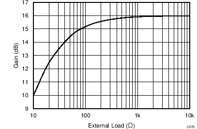
The LMH5401 has on-chip series output resistors to facilitate board layout. These resistors provide the LMH5401 extra phase margin in most applications. When the amplifier is used to drive a terminated transmission line or a controlled impedance filter, extra resistance is required to match the transmission line of the filter. In these applications, there is a 6 dB loss of gain. When the LMH5401 is used to drive loads that are not back-terminated there is a loss in gain resulting from the on-chip resistors. Figure 76 shows that loss for different load conditions. In most cases the loads are between 50 Ω and 200 Ω, where the on-chip resistor losses are 1.6 dB and 0.42 dB, respectively. Figure 77 shows the net gain realized by the amplifier for a large range of load resistances when the LMH5401 is configured for 16-dB gain.
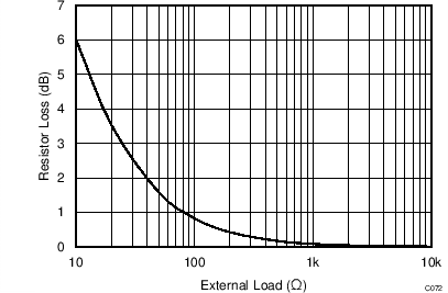
LMH5401 ai_C072_Gain_loss_bos695.pngFigure 76. Gain Loss Resulting from On-Chip Output Resistors
LMH5401 ai_C073_Gain_Load_bos695.pngFigure 77. Net Gain versus Load Resistance