SBOS730A April 2015 – May 2015 LMH6401
PRODUCTION DATA.
- 1 Features
- 2 Applications
- 3 Description
- 4 Revision History
- 5 Device Options
- 6 Pin Configuration and Functions
- 7 Specifications
- 8 Parameter Measurement Information
-
9 Detailed Description
- 9.1 Overview
- 9.2 Functional Block Diagram
- 9.3 Feature Description
- 9.4 Device Functional Modes
- 9.5 Programming
- 9.6
Register Maps
- 9.6.1 Revision ID (address = 0h, Read-Only) [default = 03h]
- 9.6.2 Product ID (address = 1h, Read-Only) [default = 00h]
- 9.6.3 Gain Control (address = 2h) [default = 20h]
- 9.6.4 Reserved (address = 3h) [default = 8Ch]
- 9.6.5 Thermal Feedback Gain Control (address = 4h) [default = 27h]
- 9.6.6 Thermal Feedback Frequency Control (address = 5h) [default = 45h]
- 10Application and Implementation
- 11Power-Supply Recommendations
- 12Layout
- 13Device and Documentation Support
- 14Mechanical, Packaging, and Orderable Information
12 Layout
12.1 Layout Guidelines
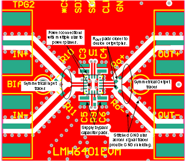
When dealing with a device with relatively high gain and bandwidth in excess of 1 GHz, certain board layout precautions must be taken to ensure stability and optimum performance. TI recommends that the LMH6401 board be multi-layered to improve thermal performance, grounding, and power-supply decoupling. The differential input and output traces must be symmetrical in order to achieve the best linearity performance.
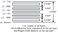
By sandwiching the power-supply layer between ground layers on either side (with thin dielectric thicknesses), parasitic capacitance between power and ground functions as a distributed, high-resonance frequency capacitor to help with power-supply decoupling. The LMH6401 evaluation board includes a total of six layers and the positive (VS+) and negative (VS–) power planes are sandwiched in the middle with a board stack-up (dielectric thickness), as shown in Figure 71, to help with supply decoupling. Both VS+ and VS– must be connected to the internal power planes through multiple vias in the immediate vicinity of the supply pins. In addition, low ESL, ceramic, 0.01-μF decoupling capacitors to the supplies are placed on the same layer as the device to provide supply decoupling.
Routing high-frequency signal traces on a PCB requires careful attention to maintain signal integrity. A board layout software package can simplify the trace thickness design to maintain impedances for controlled impedance signals. In order to isolate the affect of board parasitic on frequency response, TI recommends placing the external output matching resistors close to the amplifier output pins. A 0.01-µF bypass capacitor is also recommended close to the VOCM pins to suppress high-frequency common-mode noise. Refer to the user guide LMH6401EVM Evaluation Module (SLOU406) for more details on board layout and design.
In order to improve board mechanical reliability, the LMH6401 has square anchor pins on four corners of the package that must be soldered to the board for mechanical strength.
 Figure 71. Recommended PCB Layer Stack-Up for a Six-Layer Board
12.2 Layout Examples
 Figure 72. EVM Top Layer
 Figure 73. EVM Second Layer Showing a Solid GND Plane