JAJSFY7G February   2012  – August 2018 LMK00304

PRODUCTION DATA.  

  1. 特長
  2. アプリケーション
  3. 概要
    1.     Device Images
      1.      機能ブロック図
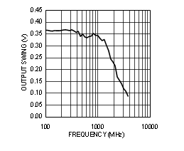
      2.      LVPECL出力スイング(VOD)と周波数との関係
  4. 改訂履歴
  5. Pin Configuration and Functions
    1.     Pin Functions
  6. Specifications
    1. 6.1 Absolute Maximum Ratings
    2. 6.2 ESD Ratings
    3. 6.3 Recommended Operating Conditions
    4. 6.4 Thermal Information
    5. 6.5 Electrical Characteristics
    6. 6.6 Typical Characteristics
  7. Parameter Measurement Information
    1. 7.1 Differential Voltage Measurement Terminology
  8. Detailed Description
    1. 8.1 Overview
    2. 8.2 Functional Block Diagram
    3. 8.3 Feature Description
      1. 8.3.1 VCC and VCCO Power Supplies
      2. 8.3.2 Clock Inputs
      3. 8.3.3 Clock Outputs
        1. 8.3.3.1 Reference Output
  9. Application and Implementation
    1. 9.1 Driving the Clock Inputs
    2. 9.2 Crystal Interface
    3. 9.3 Termination and Use of Clock Drivers
      1. 9.3.1 Termination for DC-Coupled Differential Operation
      2. 9.3.2 Termination for AC-Coupled Differential Operation
      3. 9.3.3 Termination for Single-Ended Operation
  10. 10Power Supply Recommendations
    1. 10.1 Power Supply Sequencing
    2. 10.2 Current Consumption and Power Dissipation Calculations
      1. 10.2.1 Power Dissipation Example: Worst-Case Dissipation
    3. 10.3 Power Supply Bypassing
      1. 10.3.1 Power Supply Ripple Rejection
    4. 10.4 Thermal Management
      1. 10.4.1 Support for PCB Temperature up to 105°C
  11. 11デバイスおよびドキュメントのサポート
    1. 11.1 ドキュメントのサポート
      1. 11.1.1 関連資料
    2. 11.2 ドキュメントの更新通知を受け取る方法
    3. 11.3 コミュニティ・リソース
    4. 11.4 商標
    5. 11.5 静電気放電に関する注意事項
    6. 11.6 Glossary
  12. 12メカニカル、パッケージ、および注文情報

パッケージ・オプション

メカニカル・データ(パッケージ|ピン)
サーマルパッド・メカニカル・データ
発注情報

Typical Characteristics

Unless otherwise specified: Vcc = 3.3 V, Vcco = 3.3 V, TA = 25 °C, CLKin driven differentially, input slew rate ≥ 3 V/ns. Consult Table 1 at the end of the Typical Characteristics section for graph notes.
LMK00304 30177376.gif
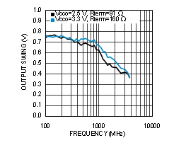
Figure 1. LVPECL Output Swing (VOD) vs. Frequency
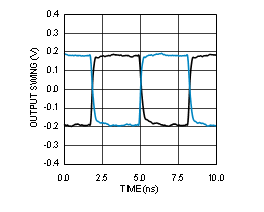
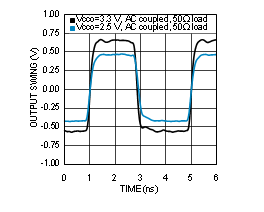
LMK00304 30177391.gif
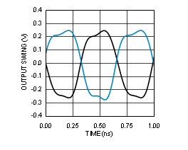
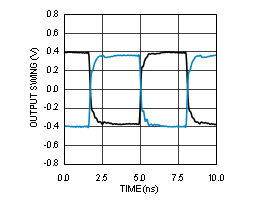
Figure 3. LVPECL Output Swing at 156.25 MHz
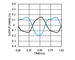
LMK00304 30177393.gif
Figure 5. LVPECL Output Swing at 1.5 GHz
LMK00304 30177398.gif
Figure 7. HCSL Output Swing at 250 MHz
LMK00304 30177377.gif
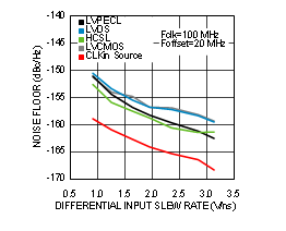
Figure 9. Noise Floor vs. CLKin Slew Rate at 100 MHz
LMK00304 SNAS577_Noise_Floor_CLKin.gif
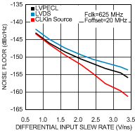
Figure 11. Noise Floor vs. CLKin Slew Rate at 625 MHz
LMK00304 30177381.gif
See Note 1 in Graph Notes table
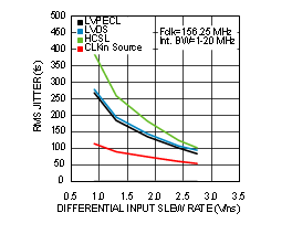
Figure 13. RMS Jitter vs. CLKin Slew Rate at 156.25 MHz
LMK00304 SNAS577_PSRR_vs_Ripple.gif
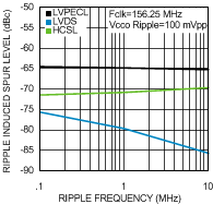
Figure 15. PSRR vs. Ripple Frequency at 156.25 MHz
LMK00304 30177385.gif
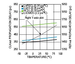
Figure 17. Propagation Delay vs. Temperature
LMK00304 30177396.png
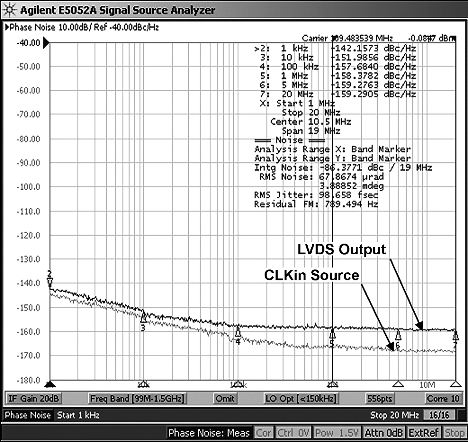
See Note 1 in Graph Notes table
Figure 19. LVDS Phase Noise at 100 MHz
LMK00304 30177331.gif
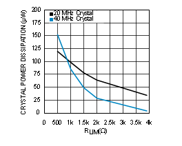
See Notes 2 and 3 in Graph Notes table
Figure 21. Crystal Power Dissipation vs. RLIM
LMK00304 30177375.gif
Figure 2. LVDS Output Swing (VOD) vs. Frequency
LMK00304 30177392.gif
Figure 4. LVDS Output Swing at 156.25 MHz
LMK00304 30177394.gif
Figure 6. LVDS Output Swing at 1.5 GHz
LMK00304 30177399.gif
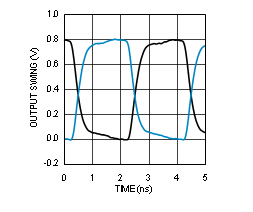
Figure 8. LVCMOS Output Swing at 250 MHz
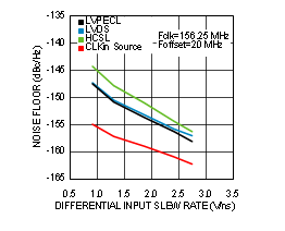
LMK00304 30177378.gif
Figure 10. Noise Floor vs. CLKin Slew Rate at 156.25 MHz
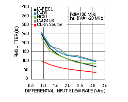
LMK00304 30177380.gif
See Note 1 in Graph Notes table
Figure 12. RMS Jitter vs. CLKin Slew Rate at 100 MHz
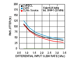
LMK00304 30177382.gif
Figure 14. RMS Jitter vs. CLKin Slew Rate at 625 MHz
LMK00304 30177384.gif
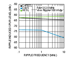
Figure 16. PSRR vs. Ripple Frequency at 312.5 MHz
LMK00304 30177395.png
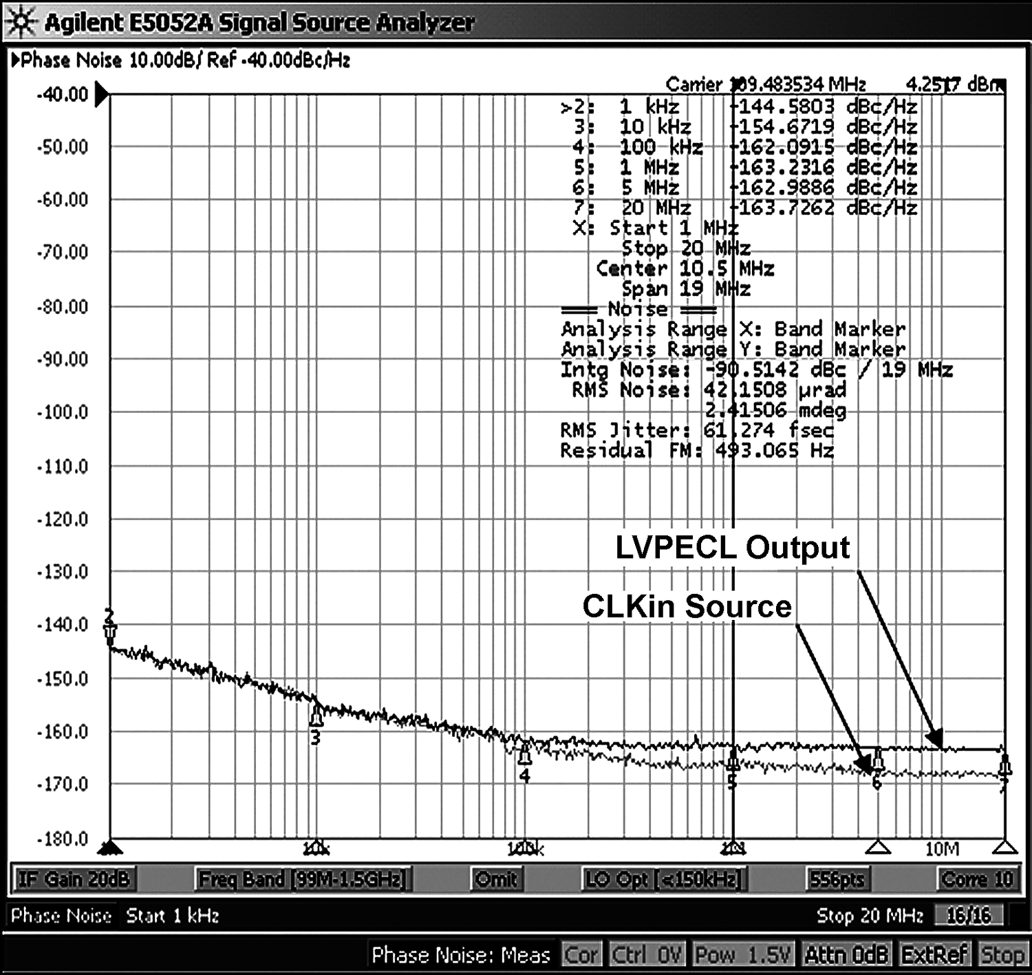
See Note 1 in Graph Notes table
Figure 18. LVPECL Phase Noise at 100 MHz
LMK00304 30177397.png
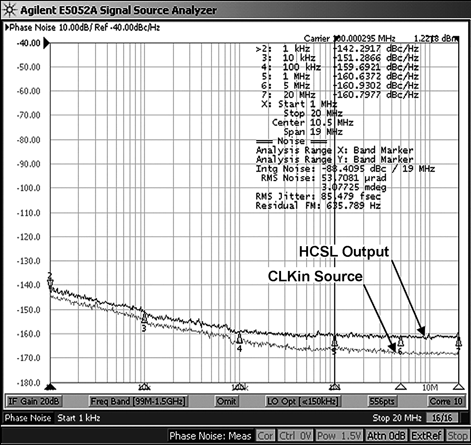
See Note 1 in Graph Notes table
Figure 20. HCSL Phase Noise at 100 MHz
LMK00304 30177332.gif
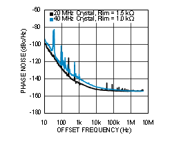
See Notes 2 and 3 in Graph Notes table
Figure 22. LVDS Phase Noise in Crystal Mode

Table 1. Graph Notes

NOTE
(1) The typical RMS jitter values in the plots show the total output RMS jitter (JOUT) for each output buffer type and the source clock RMS jitter (JSOURCE). From these values, the Additive RMS Jitter can be calculated as: JADD = SQRT(JOUT2 - JSOURCE2).
(2) 20 MHz crystal characteristics: Abracon ABL series, AT cut, CL = 18 pF , C0 = 4.4 pF measured (7 pF max), ESR = 8.5 Ω measured (40 Ω max), and Drive Level = 1 mW max (100 µW typical).
(3) 40 MHz crystal characteristics: Abracon ABLS2 series, AT cut, CL = 18 pF , C0 = 5 pF measured (7 pF max), ESR = 5 Ω measured (40 Ω max), and Drive Level = 1 mW max (100 µW typical).