SNAS642A June 2014 – July 2014 LMK00804B
PRODUCTION DATA.
- 1 Features
- 2 Applications
- 3 Description
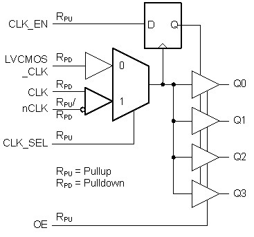
- 4 Simplified Schematic
- 5 Device Comparison Table
- 6 Pin Configuration and Functions
-
7 Specifications
- 7.1 Pin Characteristics
- 7.2 Absolute Maximum Ratings
- 7.3 Handling Ratings
- 7.4 Recommended Operating Conditions
- 7.5 Thermal Information
- 7.6 Power Supply Characteristics
- 7.7 LVCMOS / LVTTL DC Characteristics
- 7.8 Differential Input DC Characteristics
- 7.9 Electrical Characteristics (VDDO = 3.3 V ± 5%)
- 7.10 Electrical Characteristics (VDDO = 2.5 V ± 5%)
- 7.11 Electrical Characteristics (VDDO = 1.8 V ± 0.15 V)
- 7.12 Electrical Characteristics (VDDO = 1.5 V ± 5%)
- 7.13 Typical Characteristics
- 8 Parameter Measurement Information
- 9 Detailed Description
- 10Applications and Implementation
- 11Power Supply Recommendations
- 12Layout
- 13Device and Documentation Support
- 14Mechanical, Packaging, and Orderable Information
1 Features
- Four LVCMOS/LVTTL Outputs with 7 Ω Output Impedance
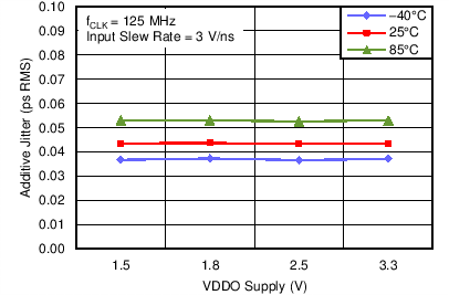
- Additive Jitter: 0.04 ps RMS (typ) @ 125 MHz
- Noise Floor: –166 dBc/Hz (typ) @ 125 MHz
- Output Frequency: 350 MHz (max)
- Output Skew: 35 ps (max)
- Part-to-Part Skew: 700 ps (max)
- Two Selectable Inputs
- CLK, nCLK Pair Accepts LVPECL, LVDS, HCSL, SSTL, LVHSTL, or LVCMOS/LVTTL
- LVCMOS_CLK Accepts LVCMOS/LVTTL
- Synchronous Clock Enable
- Core/Output Power Supplies:
- 3.3 V/3.3 V
- 3.3 V/2.5 V
- 3.3 V/1.8 V
- 3.3 V/1.5 V
- Package: 16-Lead TSSOP
- Industrial Temperature Range: –40ºC to +85ºC
2 Applications
- Wireless and Wired Infrastructure
- Networking and Data Communications
- Servers and Computing
- Medical Imaging
- Portable Test and Measurement
- High-End A/V
3 Description
The LMK00804B is a low skew, high performance clock fanout buffer which can distribute up to four LVCMOS/LVTTL outputs (3.3-V, 2.5-V, 1.8-V, or 1.5-V levels) from one of two selectable inputs, which can accept differential or single-ended inputs. The clock enable input is synchronized internally to eliminate runt or glitch pulses on the outputs when the clock enable terminal is asserted or de-asserted. The outputs are held in logic low state when the clock is disabled. A separate output enable terminal controls whether the outputs are active state or high-impedance state. The low additive jitter and phase noise floor, and guaranteed output and part-to-part skew characteristics make the LMK00804B ideal for applications demanding high performance and repeatability.
See also Device Comparison Table for descriptions of CDCLVC1310 and LMK00725 parts.
Device Information(1)
| PART NUMBER | PACKAGE | BODY SIZE (NOM) |
|---|---|---|
| LMK00804B | TSSOP (16) | 5.00 mm × 4.40 mm |
- For all available packages, see the orderable addendum at the end of the datasheet.
4 Simplified Schematic
Additive Jitter vs VDDO Supply and Temperature