SNAS674B September 2015 – February 2017 LMK61E2
PRODUCTION DATA.
- 1 Features
- 2 Applications
- 3 Description
- 4 Revision History
- 5 Pin Configuration and Functions
-
6 Specifications
- 6.1 Absolute Maximum Ratings
- 6.2 ESD Ratings
- 6.3 Recommended Operating Conditions
- 6.4 Thermal Information
- 6.5 Electrical Characteristics - Power Supply
- 6.6 LVPECL Output Characteristics
- 6.7 LVDS Output Characteristics
- 6.8 HCSL Output Characteristics
- 6.9 OE Input Characteristics
- 6.10 ADD Input Characteristics
- 6.11 Frequency Tolerance Characteristics
- 6.12 Power-On/Reset Characteristics (VDD)
- 6.13 I2C-Compatible Interface Characteristics (SDA, SCL)
- 6.14 PSRR Characteristics
- 6.15 Other Characteristics
- 6.16 PLL Clock Output Jitter Characteristics
- 6.17 Typical 156.25-MHz Output Phase Noise Characteristics
- 6.18 Typical 161.1328125 MHz Output Phase Noise Characteristics
- 6.19 Additional Reliability and Qualification
- 6.20 Typical Characteristics
- 7 Parameter Measurement Information
-
8 Detailed Description
- 8.1 Overview
- 8.2 Functional Block Diagram
- 8.3
Feature Description
- 8.3.1 Device Block-Level Description
- 8.3.2 Device Configuration Control
- 8.3.3 Register File Reference Convention
- 8.3.4 Configuring the PLL
- 8.3.5 Integrated Oscillator
- 8.3.6 Reference Doubler
- 8.3.7 Phase Frequency Detector
- 8.3.8 Feedback Divider (N)
- 8.3.9 Fractional Circuitry
- 8.3.10 Charge Pump
- 8.3.11 Loop Filter
- 8.3.12 VCO Calibration
- 8.3.13 High-Speed Output Divider
- 8.3.14 High-Speed Clock Output
- 8.3.15 Device Status
- 8.4 Device Functional Modes
- 8.5 Programming
- 8.6 EEPROM Map
- 8.7
Register Map
- 8.7.1
Register Descriptions
- 8.7.1.1 VNDRID_BY1 Register; R0
- 8.7.1.2 VNDRID_BY0 Register; R1
- 8.7.1.3 PRODID Register; R2
- 8.7.1.4 REVID Register; R3
- 8.7.1.5 SLAVEADR Register; R8
- 8.7.1.6 EEREV Register; R9
- 8.7.1.7 DEV_CTL Register; R10
- 8.7.1.8 XO_CAPCTRL_BY1 Register; R16
- 8.7.1.9 XO_CAPCTRL_BY0 Register; R17
- 8.7.1.10 DIFFCTL Register; R21
- 8.7.1.11 OUTDIV_BY1 Register; R22
- 8.7.1.12 OUTDIV_BY0 Register; R23
- 8.7.1.13 PLL_NDIV_BY1 Register; R25
- 8.7.1.14 PLL_NDIV_BY0 Register; R26
- 8.7.1.15 PLL_FRACNUM_BY2 Register; R27
- 8.7.1.16 PLL_FRACNUM_BY1 Register; R28
- 8.7.1.17 PLL_FRACNUM_BY0 Register; R29
- 8.7.1.18 PLL_FRACDEN_BY2 Register; R30
- 8.7.1.19 PLL_FRACDEN_BY1 Register; R31
- 8.7.1.20 PLL_FRACDEN_BY0 Register; R32
- 8.7.1.21 PLL_MASHCTRL Register; R33
- 8.7.1.22 PLL_CTRL0 Register; R34
- 8.7.1.23 PLL_CTRL1 Register; R35
- 8.7.1.24 PLL_LF_R2 Register; R36
- 8.7.1.25 PLL_LF_C1 Register; R37
- 8.7.1.26 PLL_LF_R3 Register; R38
- 8.7.1.27 PLL_LF_C3 Register; R39
- 8.7.1.28 PLL_CALCTRL Register; R42
- 8.7.1.29 NVMSCRC Register; R47
- 8.7.1.30 NVMCNT Register; R48
- 8.7.1.31 NVMCTL Register; R49
- 8.7.1.32 MEMADR Register; R51
- 8.7.1.33 NVMDAT Register; R52
- 8.7.1.34 RAMDAT Register; R53
- 8.7.1.35 NVMUNLK Register; R56
- 8.7.1.36 INT_LIVE Register; R66
- 8.7.1.37 SWRST Register; R72
- 8.7.1
Register Descriptions
-
9 Application and Implementation
- 9.1 Application Information
- 9.2
Typical Applications
- 9.2.1 Jitter Considerations in Serdes Systems
- 9.2.2 Frequency Margining
- 9.2.3 Design Requirements
- 10Power Supply Recommendations
- 11Layout
- 12Device and Documentation Support
- 13Mechanical, Packaging, and Orderable Information
6 Specifications
6.1 Absolute Maximum Ratings
over operating free-air temperature range (unless otherwise noted)(1)| MIN | MAX | UNIT | ||
|---|---|---|---|---|
| VDD | Device supply voltage | –0.3 | 3.6 | V |
| VIN | Output voltage for logic inputs | –0.3 | VDD + 0.3 | V |
| VOUT | Output voltage for clock outputs | –0.3 | VDD + 0.3 | V |
| TJ | Junction temperature | 150 | °C | |
| Tstg | Storage temperature | –40 | 125 | °C |
(1) Stresses beyond those listed under Absolute Maximum Ratings may cause permanent damage to the device. These are stress ratings only, which do not imply functional operation of the device at these or any other conditions beyond those indicated under Recommended Operating Conditions. Exposure to absolute maximum-rated conditions for extended periods may affect device reliability.
6.2 ESD Ratings
| VALUE | UNIT | |||
|---|---|---|---|---|
| V(ESD) | Electrostatic discharge | Human-body model (HBM), per ANSI/ESDA/JEDEC JS-001(1) | ±2000 | V |
| Charged-device model (CDM), per JEDEC specification JESD22-C101(2) | ±500 | |||
(1) JEDEC document JEP155 states that 500 V HBM allows safe manufacturing with a standard ESD control process.
(2) JEDEC document JEP157 states that 250 V CDM allows safe manufacturing with a standard ESD control process.
6.3 Recommended Operating Conditions
over operating free-air temperature range (unless otherwise noted)| MIN | NOM | MAX | UNIT | ||
|---|---|---|---|---|---|
| VDD | Device supply voltage | 3.135 | 3.3 | 3.465 | V |
| TA | Ambient temperature | –40 | 25 | 85 | °C |
| TJ | Junction temperature | 125 | °C | ||
| tRAMP | VDD power-up ramp time | 0.1 | 100 | ms | |
6.4 Thermal Information
| THERMAL METRIC(1) | LMK61E2 (2) (3) (4) | UNIT | |||
|---|---|---|---|---|---|
| QFM (SIA) | |||||
| 8 PINS | |||||
| AIRFLOW (LFM) 0 | AIRFLOW (LFM) 200 | AIRFLOW (LFM) 400 | |||
| RθJA | Junction-to-ambient thermal resistance | 54 | 44 | 41.2 | °C/W |
| RθJC(top) | Junction-to-case (top) thermal resistance | 34 | n/a | n/a | °C/W |
| RθJB | Junction-to-board thermal resistance | 36.7 | n/a | n/a | °C/W |
| ψJT | Junction-to-top characterization parameter | 11.2 | 16.9 | 21.9 | °C/W |
| ψJB | Junction-to-board characterization parameter | 36.7 | 37.8 | 38.9 | °C/W |
| RθJC(bot) | Junction-to-case (bottom) thermal resistance | n/a | n/a | n/a | °C/W |
(1) For more information about traditional and new thermal metrics, see the Semiconductor and IC Package Thermal Metrics application report.
(2) The package thermal resistance is calculated on a 4-layer JEDEC board.
(3) Connected to GND with 3 thermal vias (0.3-mm diameter).
(4) ψJB (junction-to-board) is used when the main heat flow is from the junction to the GND pad. See the Layout section for more information on ensuring good system reliability and quality.
6.5 Electrical Characteristics - Power Supply(1)
VDD = 3.3 V ± 5%, TA = –40°C to 85°C| PARAMETER | TEST CONDITIONS | MIN | TYP | MAX | UNIT | |
|---|---|---|---|---|---|---|
| IDD | Device current consumption | LVPECL(2) | 162 | 208 | mA | |
| LVDS | 152 | 196 | ||||
| HCSL | 155 | 196 | ||||
| IDD-PD | Device current consumption when output is disabled | OE = GND | 136 | mA | ||
(1) See Parameter Measurement Information for relevant test conditions.
(2) On-chip power dissipation should exclude 40 mW, dissipated in the 150-Ω termination resistors, from total power dissipation.
6.6 LVPECL Output Characteristics(1)
VDD = 3.3 V ± 5%, TA = –40°C to 85°C| PARAMETER | TEST CONDITIONS | MIN | TYP | MAX | UNIT | |
|---|---|---|---|---|---|---|
| fOUT | Output frequency(2) | 10 | 1000 | MHz | ||
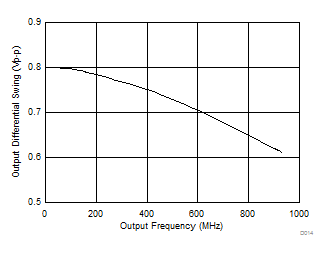
| VOD | Output voltage swing (VOH – VOL)(2) |
700 | 800 | 1200 | mV | |
| VOUT, DIFF, PP | Differential output peak-to-peak swing | 2 × |VOD| | V | |||
| VOS | Output common-mode voltage | VDD – 1.55 | V | |||
| tR / tF | Output rise/fall time (20% to 80%)(3) | 120 | 200 | ps | ||
| PN-Floor | Output phase noise floor (fOFFSET > 10 MHz) | 156.25 MHz | –165 | dBc/Hz | ||
| ODC | Output duty cycle(3) | 45% | 55% | |||
(1) See Parameter Measurement Information for relevant test conditions.
(2) An output frequency over fOUT max spec is possible, but output swing may be less than VOD min spec.
(3) Ensured by characterization.
6.7 LVDS Output Characteristics(1)
VDD = 3.3 V ± 5%, TA = –40°C to 85°C| PARAMETER | TEST CONDITIONS | MIN | TYP | MAX | UNIT | |
|---|---|---|---|---|---|---|
| fOUT | Output frequency(1) | 10 | 900 | MHz | ||
| VOD | Output voltage swing (VOH – VOL)(1) |
300 | 390 | 480 | mV | |
| VOUT, DIFF, PP | Differential output peak-to-peak swing | 2 × |VOD| | V | |||
| VOS | Output common-mode voltage | 1.2 | V | |||
| tR / tF | Output rise/fall time (20% to 80%)(2) | 150 | 250 | ps | ||
| PN-Floor | Output phase noise floor (fOFFSET > 10 MHz) | 156.25 MHz | –162 | dBc/Hz | ||
| ODC | Output duty cycle(2) | 45% | 55% | |||
| ROUT | Differential output impedance | 125 | Ω | |||
(1) An output frequency over fOUT max spec is possible, but output swing may be less than VOD min spec.
(2) Ensured by characterization.
6.8 HCSL Output Characteristics(1)
VDD = 3.3 V ± 5%, TA = –40°C to 85°C| PARAMETER | TEST CONDITIONS | MIN | TYP | MAX | UNIT | |
|---|---|---|---|---|---|---|
| fOUT | Output frequency | 10 | 400 | MHz | ||
| VOH | Output high voltage | 600 | 850 | mV | ||
| VOL | Output low voltage | –100 | 100 | mV | ||
| VCROSS | Absolute crossing voltage(2)(3) | 250 | 475 | mV | ||
| VCROSS-DELTA | Variation of VCROSS(2)(3) | 0 | 140 | mV | ||
| dV/dt | Slew rate(4) | 0.8 | 2 | V/ns | ||
| PN-Floor | Output phase noise floor (fOFFSET > 10 MHz) | 100 MHz | –164 | dBc/Hz | ||
| ODC | Output duty cycle(4) | 45% | 55% | |||
(1) See Parameter Measurement Information for relevant test conditions.
(2) Measured from –150 mV to +150 mV on the differential waveform with the 300-mVpp measurement window centered on the differential zero crossing.
(3) Ensured by design.
(4) Ensured by characterization.
6.9 OE Input Characteristics
VDD = 3.3 V ± 5%, TA = –40°C to 85°C| PARAMETER | TEST CONDITIONS | MIN | TYP | MAX | UNIT | |
|---|---|---|---|---|---|---|
| VIH | Input high voltage | 1.4 | V | |||
| VIL | Input low voltage | 0.6 | V | |||
| IIH | Input high current | VIH = VDD | –40 | 40 | µA | |
| IIL | Input low current | VIL = GND | –40 | 40 | µA | |
| CIN | Input capacitance | 2 | pF | |||
6.10 ADD Input Characteristics
VDD = 3.3 V ± 5%, TA = –40°C to 85°C| PARAMETER | TEST CONDITIONS | MIN | TYP | MAX | UNIT | |
|---|---|---|---|---|---|---|
| VIH | Input high voltage | 1.4 | V | |||
| VIL | Input low voltage | 0.4 | V | |||
| IIH | Input high current | VIH = VDD | –40 | 40 | µA | |
| IIL | Input low current | VIL = GND | –40 | 40 | µA | |
| CIN | Input capacitance | 2 | pF | |||
6.11 Frequency Tolerance Characteristics(1)
VDD = 3.3 V ± 5%, TA = –40°C to 85°C| PARAMETER | TEST CONDITIONS | MIN | TYP | MAX | UNIT | |
|---|---|---|---|---|---|---|
| fT | Total frequency tolerance | All output formats, frequency bands and device junction temperature up to 125°C; includes initial freq tolerance, temperature & supply voltage variation, solder reflow and aging (10 years) | –50 | 50 | ppm | |
(1) Ensured by characterization.
6.12 Power-On/Reset Characteristics (VDD)
VDD = 3.3 V ± 5%, TA = –40°C to 85°C| PARAMETER | TEST CONDITIONS | MIN | TYP | MAX | UNIT | |
|---|---|---|---|---|---|---|
| VTHRESH | Threshold voltage(1) | 2.72 | 2.95 | V | ||
| VDROOP | Allowable voltage droop(2) | 0.1 | V | |||
| tSTARTUP | Start-up time (1) | Time elapsed from VDD at 3.135 V to output enabled | 10 | ms | ||
| tOE-EN | Output enable time(2) | Time elapsed from OE at VIH to output enabled | 50 | µs | ||
| tOE-DIS | Output disable time(2) | Time elapsed from OE at VIL to output disabled | 50 | µs | ||
(1) Ensured by characterization.
(2) Ensured by design.
6.13 I2C-Compatible Interface Characteristics (SDA, SCL)(1)(2)
VDD = 3.3 V ± 5%, TA = –40°C to 85°C| PARAMETER | TEST CONDITIONS | MIN | TYP | MAX | UNIT | |
|---|---|---|---|---|---|---|
| VIH | Input high voltage | 1.2 | V | |||
| VIL | Input low voltage | 0.6 | V | |||
| IIH | Input leakage | –40 | 40 | µA | ||
| CIN | Input capacitance | 2 | pF | |||
| COUT | Input capacitance | 400 | pF | |||
| VOL | Output low voltage | IOL = 3 mA | 0.6 | V | ||
| fSCL | I2C clock rate | 100 | 400 | kHz | ||
| tSU_STA | START condition setup time | SCL high before SDA low | 0.6 | µs | ||
| tH_STA | START condition hold time | SCL low after SDA low | 0.6 | µs | ||
| tPH_SCL | SCL pulse width high | 0.6 | µs | |||
| tPL_SCL | SCL pulse width low | 1.3 | µs | |||
| tH_SDA | SDA hold time | SDA valid after SCL low | 0 | 0.9 | µs | |
| tSU_SDA | SDA setup time | 115 | ns | |||
| tR_IN / tF_IN | SCL/SDA input rise and fall time | 300 | ns | |||
| tF_OUT | SDA output fall time | CBUS = 10 pF to 400 pF | 250 | ns | ||
| tSU_STOP | STOP condition setup time | 0.6 | µs | |||
| tBUS | Bus free time between STOP and START | 1.3 | µs | |||
(1) Total capacitive load for each bus line ≤ 400 pF.
(2) Ensured by design.
6.14 PSRR Characteristics(1)
VDD = 3.3 V, TA = 25°C, PLL bandwidth = 400 kHz, VCO Frequency = 5 GHz (Integer-N PLL), Output Divider = 32, Output Type = LVPECL/LVDS/HCSL| PARAMETER | TEST CONDITIONS | MIN | TYP | MAX | UNIT | |
|---|---|---|---|---|---|---|
| PSRR | Spurs induced by 50-mV power supply ripple(2)(3) at 156.25-MHz output, all output types | Sine wave at 50 kHz | –70 | dBc | ||
| Sine wave at 100 kHz | –70 | |||||
| Sine wave at 500 kHz | –70 | |||||
| Sine wave at 1 MHz | –70 | |||||
(1) See Parameter Measurement Information for relevant test conditions.
(2) Measured maximum spur level with 50-mVpp sinusoidal signal between 50 kHz and 1 MHz applied on VDD pin
(3) DJSPUR (ps, pk-pk) = [2 × 10(SPUR/20) / (π × fOUT)] × 1e6, where PSRR or SPUR in dBc and fOUT in MHz.
6.15 Other Characteristics
VDD = 3.3 V ± 5%, TA = –40°C to 85°C| PARAMETER | TEST CONDITIONS | MIN | TYP | MAX | UNIT | |
|---|---|---|---|---|---|---|
| fVCO | VCO frequency range | 4.6 | 5.6 | GHz | ||
6.16 PLL Clock Output Jitter Characteristics(1)(3)
VDD = 3.3 V ± 5%, TA = –40°C to 85°C| PARAMETER | TEST CONDITIONS | MIN | TYP | MAX | UNIT | |
|---|---|---|---|---|---|---|
| RJ | RMS phase jitter(2)
(12 kHz – 20 MHz) (1 kHz – 5 MHz) |
fOUT ≥ 100 MHz, Integer-N PLL, All output types | 100 | 200 | fs RMS | |
| RJ | RMS phase jitter(2)
(12 kHz – 20 MHz) (1 kHz – 5 MHz) |
fOUT ≥ 100 MHz, Fractional-N PLL, All output types | 150 | 300 | fs RMS | |
(1) See Parameter Measurement Information for relevant test conditions.
(2) Ensured by characterization.
(3) Phase jitter measured with Agilent E5052 signal source analyzer using a differential-to-single ended converter (balun or buffer).
6.17 Typical 156.25-MHz Output Phase Noise Characteristics(1)(2)
VDD = 3.3 V, TA = 25°C, PLL bandwidth = 400 kHz, VCO Frequency = 5 GHz, Integer-N PLL, Output Divider = 32, Output Type = LVPECL/LVDS/HCSL| PARAMETER | OUTPUT TYPE | UNIT | |||
|---|---|---|---|---|---|
| LVPECL | LVDS | HCSL | |||
| phn10k | Phase noise at 10-kHz offset | –143 | –143 | –143 | dBc/Hz |
| Phn20k | Phase noise at 20-kHz offset | –143 | –143 | –143 | dBc/Hz |
| phn100k | Phase noise at 100-kHz offset | –144 | –144 | –144 | dBc/Hz |
| Phn200k | Phase noise at 200-kHz offset | –145 | –145 | –145 | dBc/Hz |
| phn1M | Phase noise at 1-MHz offset | –150 | –150 | –150 | dBc/Hz |
| phn2M | Phase noise at 2-MHz offset | –154 | –154 | –154 | dBc/Hz |
| phn10M | Phase noise at 10-MHz offset | –165 | –162 | –164 | dBc/Hz |
| phn20M | Phase noise at 20-MHz offset | –165 | –162 | –164 | dBc/Hz |
(1) See Parameter Measurement Information for relevant test conditions.
(2) Phase jitter measured with Agilent E5052 signal source analyzer using a differential-to-single ended converter (balun or buffer).
6.18 Typical 161.1328125 MHz Output Phase Noise Characteristics(1)(2)
VDD = 3.3 V, TA = 25°C, PLL bandwidth = 400 kHz, VCO Frequency = 5.15625 GHz, Fractional-N PLL, Output Divider = 32, Output Type = LVPECL/LVDS/HCSL| PARAMETER | OUTPUT TYPE | UNIT | |||
|---|---|---|---|---|---|
| LVPECL | LVDS | HCSL | |||
| phn10k | Phase noise at 10-kHz offset | –136 | –136 | –136 | dBc/Hz |
| phn20k | Phase noise at 20-kHz offset | –136 | –136 | –136 | dBc/Hz |
| phn100k | Phase noise at 100-kHz offset | –140 | –140 | –140 | dBc/Hz |
| phn200k | Phase noise at 200-kHz offset | –141 | –141 | –141 | dBc/Hz |
| phn1M | Phase noise at 1-MHz offset | –148 | –148 | –148 | dBc/Hz |
| phn2M | Phase noise at 2-MHz offset | –156 | –156 | –156 | dBc/Hz |
| phn10M | Phase noise at 10-MHz offset | –161 | –159 | –160 | dBc/Hz |
| phn20M | Phase noise at 20-MHz offset | –162 | –160 | –161 | dBc/Hz |
(1) See Parameter Measurement Information for relevant test conditions.
(2) Phase jitter measured with Agilent E5052 signal source analyzer using a differential-to-single ended converter (balun or buffer).
6.19 Additional Reliability and Qualification
| PARAMETER | CONDITION / TEST METHOD |
|---|---|
| Mechanical Shock | MIL-STD-202, Method 213 |
| Mechanical Vibration | MIL-STD-202, Method 204 |
| Moisture Sensitivity Level | J-STD-020, MSL3 |
6.20 Typical Characteristics
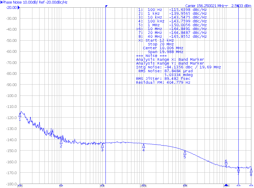 Figure 1. Closed-Loop Phase Noise of LVPECL Differential Output at 156.25 MHz
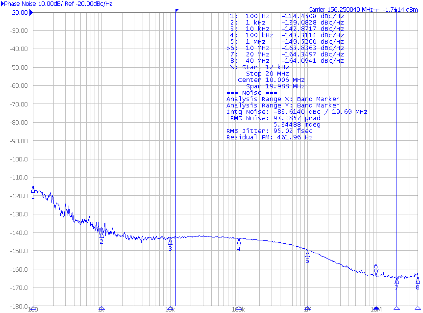
| PLL Bandwidth = 400 kHz | VCO Frequency = 5 GHz |
| Integer-N PLL | Output Divider = 32 |
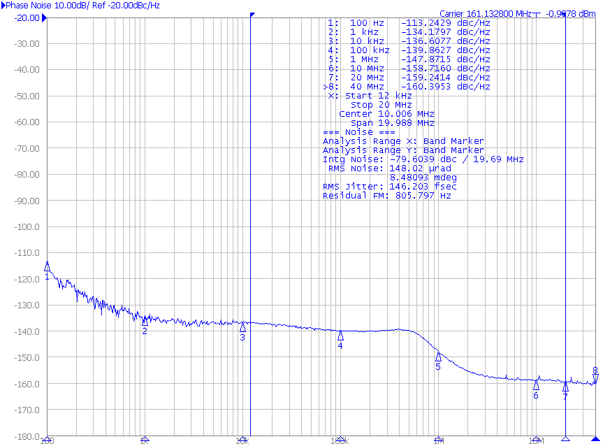
| PLL Bandwidth = 400 kHz | VCO Frequency = 5.15625 GHz |
| Fractional-N PLL | Output Divider = 32 |
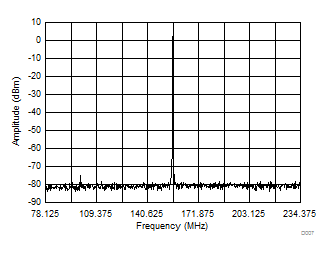
| PLL Bandwidth = 400 kHz | VCO Frequency = 5 GHz |
| Integer-N PLL | Output Divider = 32 |
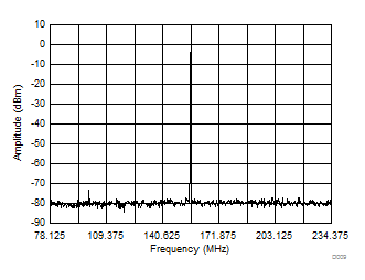
| PLL Bandwidth = 400 kHz | VCO Frequency = 5 GHz |
| Integer-N PLL | Output Divider = 32 |
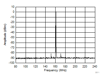
| PLL Bandwidth = 400 kHz | VCO Frequency = 5.15625 GHz |
| Fractional-N PLL | Output Divider = 32 |
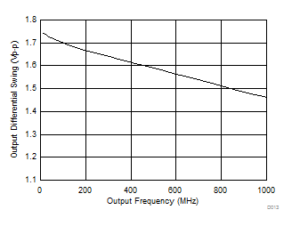
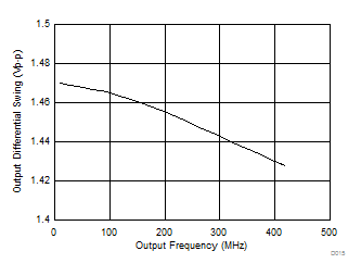
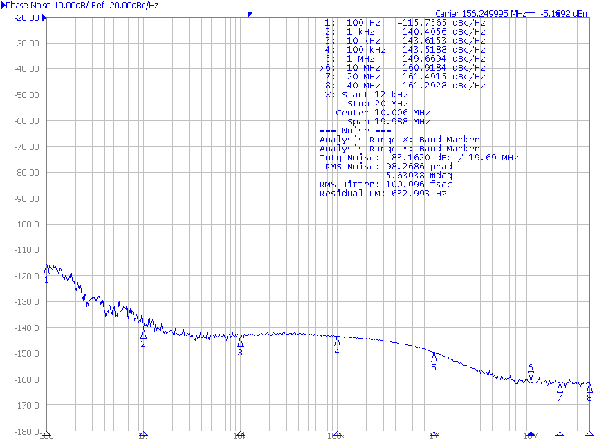
| PLL Bandwidth = 400 kHz | VCO Frequency = 5 GHz |
| Integer-N PLL | Output Divider = 32 |

| PLL Bandwidth = 400 kHz | VCO Frequency = 5.15625 GHz |
| Fractional-N PLL | Output Divider = 32 |

| PLL Bandwidth = 400 kHz | VCO Frequency = 5.15625 GHz |
| Fractional-N PLL | Output Divider = 32 |
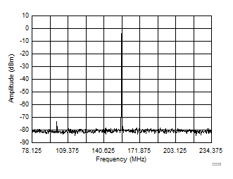
| PLL Bandwidth = 400 kHz | VCO Frequency = 5 GHz |
| Integer-N PLL | Output Divider = 32 |
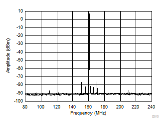
| PLL Bandwidth = 400 kHz | VCO Frequency = 5.15625 GHz |
| Fractional-N PLL | Output Divider = 32 |
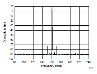
| PLL Bandwidth = 400 kHz | VCO Frequency = 5.15625 GHz |
| Fractional-N PLL | Output Divider = 32 |
