SNAS675A October 2015 – November 2015 LMK61PD0A2
PRODUCTION DATA.
- 1 Features
- 2 Applications
- 3 Description
- 4 Revision History
- 5 Device Control
- 6 Pin Configuration and Functions
-
7 Specifications
- 7.1 Absolute Maximum Ratings
- 7.2 ESD Ratings
- 7.3 Recommended Operating Conditions
- 7.4 Thermal Information
- 7.5 Electrical Characteristics - Power Supply
- 7.6 LVPECL Output Characteristics
- 7.7 LVDS Output Characteristics
- 7.8 HCSL Output Characteristics
- 7.9 OE Input Characteristics
- 7.10 OS, FS[1:0] Input Characteristics
- 7.11 Frequency Tolerance Characteristics
- 7.12 Power-On/Reset Characteristics (VDD)
- 7.13 PSRR Characteristics
- 7.14 PLL Clock Output Jitter Characteristics
- 7.15 Additional Reliability and Qualification
- 7.16 Typical Performance Characteristics
- 8 Parameter Measurement Information
- 9 Detailed Description
- 10Application and Implementation
- 11Power Supply Recommendations
- 12Layout
- 13Device and Documentation Support
- 14Mechanical, Packaging, and Orderable Information
10 Application and Implementation
NOTE
Information in the following applications sections is not part of the TI component specification, and TI does not warrant its accuracy or completeness. TI’s customers are responsible for determining suitability of components for their purposes. Customers should validate and test their design implementation to confirm system functionality.
10.1 Application Information
The LMK61PD0A2 is an ultra-low jitter pin selectable oscillator that can be used to provide reference clocks for high-speed serial links resulting in improved system performance.
10.2 Typical Application
10.2.1 Jitter Considerations in Serdes Systems
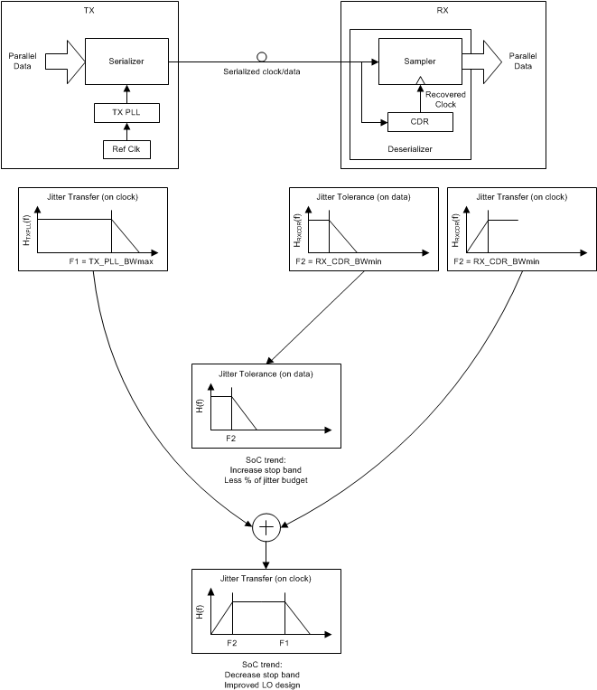
Jitter-sensitive applications such as 10 Gbps or 100 Gbps Ethernet, deploy a serial link utilizing a Serializer in the transmit section (TX) and a De-serializer in the receive section (RX). These SERDES blocks are typically embedded in an ASIC or FPGA. Estimating the clock jitter impact on the link budget requires understanding of the TX PLL bandwidth and the RX CDR bandwidth.
As can be seen in Figure 15, the pass band region between the TX low pass cutoff and RX high pass cutoff frequencies is the range over which the reference clock jitter adds without any attenuation to the jitter budget of the link. Outside of these frequencies, the SERDES link will attenuate the reference clock jitter with a 20 dB/dec or even steeper roll-off. Modern ASIC or FPGA designs have some flexibility on deciding the optimal RX CDR bandwidth and TX PLL bandwidth. These bandwidths are typically set based on what is achievable in the ASIC or FPGA process node, without increasing design complexity, and on any jitter tolerance or wander specification that needs to be met, as related to the RX CDR bandwidth.
The overall allowable jitter in a serial link is dictated by IEEE or other relevant standards. For example, IEEE802.3ba states that the maximum transmit jitter (peak-peak) for 10 Gbps Ethernet should be no more than 0.28 * UI and this equates to a 27.1516 ps, p-p for the overall allowable transmit jitter.
The jitter contributing elements are made up of the reference clock, generated potentially from a device like LMK61PD0A2, the transmit medium, transmit driver etc. Only a portion of the overall allowable transmit jitter is allocated to the reference clock, typically 20% or lower. Therefore, the allowable reference clock jitter, for a 20% clock jitter budget, is 5.43 ps, p-p.
Jitter in a reference clock is made up of deterministic jitter (arising from spurious signals due to supply noise or mixing from other outputs or from the reference input) and random jitter (usually due to thermal noise and other uncorrelated noise sources). A typical clock tree in a serial link system consists of clock generators and fanout buffers. The allowable reference clock jitter of 5.43 ps, p-p is needed at the output of the fanout buffer. Modern fanout buffers have low additive random jitter (less than 100 fs, rms) with no substantial contribution to the deterministic jitter. Therefore, the clock generator and fanout buffer contribute to the random jitter while the primary contributor to the deterministic jitter is the clock generator. Rule of thumb, for modern clock generators, is to allocate 25% of allowable reference clock jitter to the deterministic jitter and 75% to the random jitter. This amounts to an allowable deterministic jitter of 1.36 ps, p-p and an allowable random jitter of 4.07 ps, p-p. For serial link systems that need to meet a bit error rate (BER) of 10-12, the allowable random jitter in root-mean-square is 0.29 ps, rms. This is calculated by dividing the p-p jitter by 14 for a BER of 10-12. Accounting for random jitter from the fanout buffer, the random jitter needed from the clock generator is 0.27 ps, rms. This is calculated by the root-mean-square subtraction from the desired jitter at the fanout buffer's output assuming 100 fs, rms of additive jitter from the fanout buffer.
With careful frequency planning techniques, like spur optimization (covered in the Spur Mitigation Techniques section) and on-chip LDOs to suppress supply noise, the LMK61PD0A2 is able to generate clock outputs with deterministic jitter that is below 1 ps, p-p and random jitter that is below 0.2 ps, rms. This gives the serial link system with additional margin on the allowable transmit jitter resulting in a BER better than 10-12.
 Figure 15. Dependence of Clock Jitter in Serial Links