SNAS675A October 2015 – November 2015 LMK61PD0A2
PRODUCTION DATA.
- 1 Features
- 2 Applications
- 3 Description
- 4 Revision History
- 5 Device Control
- 6 Pin Configuration and Functions
-
7 Specifications
- 7.1 Absolute Maximum Ratings
- 7.2 ESD Ratings
- 7.3 Recommended Operating Conditions
- 7.4 Thermal Information
- 7.5 Electrical Characteristics - Power Supply
- 7.6 LVPECL Output Characteristics
- 7.7 LVDS Output Characteristics
- 7.8 HCSL Output Characteristics
- 7.9 OE Input Characteristics
- 7.10 OS, FS[1:0] Input Characteristics
- 7.11 Frequency Tolerance Characteristics
- 7.12 Power-On/Reset Characteristics (VDD)
- 7.13 PSRR Characteristics
- 7.14 PLL Clock Output Jitter Characteristics
- 7.15 Additional Reliability and Qualification
- 7.16 Typical Performance Characteristics
- 8 Parameter Measurement Information
- 9 Detailed Description
- 10Application and Implementation
- 11Power Supply Recommendations
- 12Layout
- 13Device and Documentation Support
- 14Mechanical, Packaging, and Orderable Information
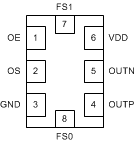
6 Pin Configuration and Functions
SIA Package
8 pin QFM

Table 3. Pin Functions
| PIN | I/O | DESCRIPTION | |
|---|---|---|---|
| NAME | NO. | ||
| POWER | |||
| GND | 3 | Ground | Device Ground. |
| VDD | 6 | Analog | 3.3 V Power Supply. |
| OUTPUT BLOCK | |||
| OUTP, OUTN | 4, 5 | Universal | Differential Output Pair (LVPECL, LVDS or HCSL). |
| DIGITAL CONTROL / INTERFACES | |||
| FS[1:0] | 7, 8 | LVCMOS | Output Frequency Select. Refer toTable 1. |
| OE | 1 | LVCMOS | Output Enable (internal pullup). Refer toTable 2. |
| OS | 3 | LVCMOS | Output Type Select. Refer toTable 2. |