SNOSA87C October 2003 – October 2016 LMV116 , LMV118
PRODUCTION DATA.
8 Application and Implementation
NOTE
Information in the following applications sections is not part of the TI component specification, and TI does not warrant its accuracy or completeness. TI’s customers are responsible for determining suitability of components for their purposes. Customers should validate and test their design implementation to confirm system functionality.
8.1 Application Information
The LMV11x rail-to-rail output voltage feedback amplifiers offer high-speed (45 MHz) operation with low input voltage (2.7 V). Output voltage range extends to within 20 mV of either supply rail, allowing wide dynamic range especially in low voltage applications. Even with low supply current of 600 μA, output current capability is kept at a respectable ±20 mA. For portable applications, the LMV118 provides shutdown capability while keeping the turnoff current to 15 μA. Both turnon and turnoff characteristics are well behaved with minimal output fluctuations during transitions which enables the use of LMV118 in multiplexing applications.
8.2 Typical Application: 2.7-V Single Supply 2:1 MUX
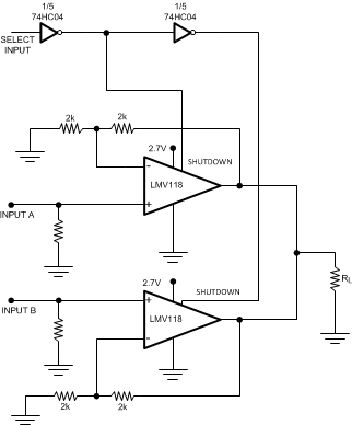
The schematic shown in Figure 23 functions as a 2:1 MUX operating on a single 2.7-V power supply, by utilizing the shutdown feature of the LMV118. Select input signal is connected to the shutdown pin of the first LMV118 through 74HC04 inverter. This signal is connected to the shutdown pin of the second LMV118 through another inverter. With this setup one of the LMV118 operational amplifiers is always in shutdown mode while the other is in active mode.
 Figure 23. 2:1 MUX Operating Off a 2.7-V Single Supply
8.2.1 Design Requirements
For typical operational-amplifier applications, use the parameters listed in Table 1.
Table 1. Design Parameters
| DESIGN PARAMETER | EXAMPLE VALUE |
|---|---|
| Supply voltage | 2.7 V |
| Linear output current | ±20 mA (typical) |
| PSRR | 85 dB (typical) |
8.2.2 Detailed Design Procedure
It is important to carefully select the values of the external resistors. Choosing large valued external resistors affects the closed-loop behavior of the stage because of the interaction of these resistors with parasitic capacitances. These capacitors could be inherent to the device or a by-product of the board layout and component placement. Either way, keeping the resistor values lower diminishes this interaction. On the other hand, choosing very low-value resistors could load down nodes and contribute to higher overall power dissipation.
8.2.3 Application Curve
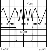
Figure 24 shows the MUX output when selecting between a 1-MHz sine and a 250-kHz triangular waveform.
As can be seen in Figure 24, the output is well behaved, and there are no spikes or glitches due to the switching. Switching times are approximately around 500 ns based on the time when the output is considered valid.
 Figure 24. 2:1 MUX Output