SNOSA87C October 2003 – October 2016 LMV116 , LMV118
PRODUCTION DATA.
7 Detailed Description
7.1 Overview
The LMV116 and LMV118 are based on TI’s proprietary VIP10 dielectrically isolated bipolar process.
The LMV116 and LMV118 architecture features the following:
- Complementary bipolar devices with exceptionally high ft (approximately 8 GHz) even under low supply voltage (2.7 V) and low collector bias current.
- Common emitter push-pull output stage capable of 20-mA output current (at 0.5 V from the supply rails) while consuming only 600 μA of total supply current. This architecture allows output to reach within milli-volts of either supply rail at light loads.
- Consistent performance from any supply voltage (2.7 V to 10 V) with little variation with supply voltage for the most important specifications (for example, BW, SR, IOUT, etc.)
7.2 Functional Block Diagram

7.3 Feature Description
The amplifier's differential inputs consist of a non-inverting input (+IN) and an inverting input (–IN). The amplifier amplifies only the difference in voltage between the two inputs, which is called the differential input voltage. The output voltage of the op-amp VOUT is given by Equation 1:
where
- AVOL is the open-loop gain of the amplifier, typically around 85 dB.
7.4 Device Functional Modes
7.4.1 Quasi-Saturated State
When the output swing approaches either supply rail, the output transistor enters a quasi-saturated state. A subtle effect of this operational region is that there is an increase in supply current in this state (up to 1 mA). The onset of quasi-saturation region is a function of output loading (current) and varies from 100 mV at no load to about 1 V when output is delivering 20 mA, as measured from supplies. Both input common mode voltage and output voltage level affect the supply current (see Typical Characteristics for plot).
7.4.2 Micro-Power Shutdown
The LMV118 can be shut down to save power and reduce its supply current to less than the 50 μA specified by applying a voltage to the SD pin. The SD pin is active high and needs to be tied to V− for normal operation. This input is low current (< 20-μA, 4-pF equivalent capacitance) and a resistor to V− (≤ 20 kΩ) results in normal operation. Shutdown is specified when SD pin is 0.4 V or less from V+ at any operating supply voltage and temperature.
In the shutdown mode, essentially all internal device biasing is turned off in order to minimize supply current flow, and the output goes into Hi-Z (high impedance) mode. Complete device turnon and turnoff times vary considerably relative to the output loading conditions, output voltage, and input impedance, but is generally limited to less than 1 μs (see Electrical Characteristics: 2.7 V, Electrical Characteristics: 5 V, and Electrical Characteristics: ±5 V)
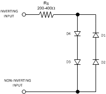
During shutdown, the input stage has an equivalent circuit as shown in Figure 20.
 Figure 20. Input Stage Shutdown Equivalent Circuit
As can be seen from Figure 20, in shutdown there may be current flow through the internal diodes shown, caused by input potential, if present. This current may flow through the external feedback resistor and result in an apparent output signal. In most shutdown applications the presence of this output is inconsequential. However, if the output is forced by another device such as in a multiplexer, the other device must conduct the current described in order to maintain the output potential.
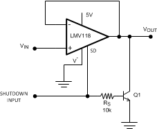
To keep the output at or near ground during shutdown when there is no other device to hold the output low, a switch (transistor) could be used to shunt the output to ground. Figure 21 shows a circuit where a NPN bipolar is used to keep the output near ground (approximately 80 mV):
 Figure 21. Active Pulldown Schematic
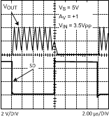
Figure 22 shows the output waveform.
 Figure 22. Output Held Low by Active Pulldown Circuit
If bipolar transistor power dissipation is not tolerable, the switch can be done by an N-channel enhancement-mode MOSFET.