JAJSAE5H February 2007 – August 2016 LMV551 , LMV552 , LMV554
PRODUCTION DATA.
- 1 特長
- 2 アプリケーション
- 3 概要
- 4 改訂履歴
- 5 Pin Configuration and Functions
- 6 Specifications
- 7 Detailed Description
- 8 Application and Implementation
- 9 Power Supply Recommendations
- 10Layout
- 11デバイスおよびドキュメントのサポート
- 12メカニカル、パッケージ、および注文情報
パッケージ・オプション
メカニカル・データ(パッケージ|ピン)
サーマルパッド・メカニカル・データ
発注情報
7 Detailed Description
7.1 Overview
The LMV55x are high performance, low power operational amplifiers implemented with TI’s advanced VIP50 process. They feature 3 MHz of bandwidth while consuming only 37 µA of current per amplifier, which is an exceptional bandwidth to power ratio in this op amp class. These amplifiers are unity gain stable and provide an excellent solution for low power applications requiring a wide bandwidth.
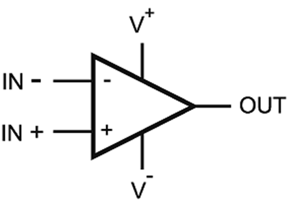
7.2 Functional Block Diagram

7.3 Feature Description
The differential inputs of the amplifier consist of a noninverting input (+IN) and an inverting input (–IN). The amplifier amplifies only the difference in voltage between the two inputs, which is called the differential input voltage. The output voltage of the op-amp VOUT is given by Equation 1:
where
- AOL is the open-loop gain of the amplifier, typically around 100 dB (100,000x, or 10 uV per volt).
7.3.1 Low Voltage and Low Power Operation
The LMV55x have performance ensured at supply voltages of 3 V and 5 V and are ensured to be operational at all supply voltages from 2.7 V to 5.5 V. For this supply voltage range, the LMV55x draw the extremely low supply current of less than 37 μA per amp.
7.3.2 Wide Bandwidth
The bandwidth to power ratio of 3 MHz to 37 μA per amplifier is one of the best bandwidth to power ratios ever achieved. This makes these devices ideal for low power signal processing applications such as portable media players and instrumentation.
7.3.3 Low Input Referred Noise
The LMV55x provide a flatband input referred voltage noise density of 70 nV/√Hz , which is significantly better than the noise performance expected from an ultra low power op amp. They also feature the exceptionally low 1/f noise corner frequency of 4 Hz. This noise specification makes the LMV55x ideal for low power applications such as PDAs and portable sensors.
7.3.4 Ground Sensing and Rail-to-Rail Output
The LMV55x each have a rail-to-rail output stage, which provides the maximum possible output dynamic range. This is especially important for applications requiring a large output swing. The input common mode range includes the negative supply rail which allows direct sensing at ground in a single supply operation.
7.3.5 Small Size
The small footprints of the LMV55x packages save space on printed circuit boards, and enable the design of smaller and more compact electronic products. Long traces between the signal source and the op amp make the signal path susceptible to noise. By using a physically smaller package, the amplifiers can be placed closer to the signal source, reducing noise pickup and enhancing signal integrity.
7.4 Device Functional Modes
7.4.1 Stability Of Op Amp Circuits
7.4.1.1 Stability and Capacitive Loading
As seen in the Phase Margin vs Capacitive Load graph, the phase margin reduces significantly for CL greater than 100 pF. This is because the op amp is designed to provide the maximum bandwidth possible for a low supply current. Stabilizing them for higher capacitive loads would have required either a drastic increase in supply current, or a large internal compensation capacitance, which would have reduced the bandwidth of the op amp. Hence, if the LMV55x are to be used for driving higher capacitive loads, they must be externally compensated.
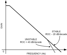
 Figure 26. Gain vs Frequency for an Op Amp
An op amp, ideally, has a dominant pole close to DC, which causes its gain to decay at the rate of 20 dB/decade with respect to frequency. If this rate of decay, also known as the rate of closure (ROC), remains the same until the op amp’s unity gain bandwidth, the op amp is stable. If, however, a large capacitance is added to the output of the op amp, it combines with the output impedance of the op amp to create another pole in its frequency response before its unity gain frequency (Figure 26). This increases the ROC to 40 dB/ decade and causes instability.
In such a case a number of techniques can be used to restore stability to the circuit. The idea behind all these schemes is to modify the frequency response such that it can be restored to an ROC of 20 dB/decade, which ensures stability.
7.4.1.1.1 In the Loop Compensation
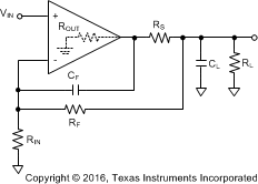
Figure 27 illustrates a compensation technique, known as ‘in the loop’ compensation, that employs an RC feedback circuit within the feedback loop to stabilize a non-inverting amplifier configuration. A small series resistance, RS, is used to isolate the amplifier output from the load capacitance, CL, and a small capacitance, CF, is inserted across the feedback resistor to bypass CL at higher frequencies.
 Figure 27. In the Loop Compensation
The values for RS and CF are decided by ensuring that the zero attributed to CF lies at the same frequency as the pole attributed to CL. This ensures that the effect of the second pole on the transfer function is compensated for by the presence of the zero, and that the ROC is maintained at 20 dB/decade. For the circuit shown in Figure 27 the values of RS and CF are given by Equation 2. Values of RS and CF required for maintaining stability for different values of CL, as well as the phase margins obtained, are shown in Table 1. RF, RIN, and RL are to be 10 kΩ, while ROUT is 340Ω.

Table 1. Phase Margins
| CL (pF) | RS (Ω) | CF (pF) | PHASE MARGIN (°) |
|---|---|---|---|
| 50 | 340 | 8 | 47 |
| 100 | 340 | 15 | 42 |
| 150 | 340 | 22 | 40 |
Although this methodology provides circuit stability for any load capacitance, it does so at the price of bandwidth. The closed loop bandwidth of the circuit is now limited by RF and CF.
7.4.1.1.2 Compensation by External Resistor
In some applications it is essential to drive a capacitive load without sacrificing bandwidth. In such a case, in the loop compensation is not viable. A simpler scheme for compensation is shown in Figure 28. A resistor, RISO, is placed in series between the load capacitance and the output. This introduces a zero in the circuit transfer function, which counteracts the effect of the pole formed by the load capacitance and ensures stability. The value of RISO to be used should be decided depending on the size of CL and the level of performance desired. Values ranging from 5 Ω to 50 Ω are usually sufficient to ensure stability. A larger value of RISO results in a system with less ringing and overshoot, but also limits the output swing and the short-circuit current of the circuit.
 Figure 28. Compensation by Isolation Resistor