SNOSC70C April 2012 – July 2016 LMV601 , LMV602 , LMV604
PRODUCTION DATA.
- 1 Features
- 2 Applications
- 3 Description
- 4 Revision History
- 5 Pin Configuration and Functions
-
6 Specifications
- 6.1 Absolute Maximum Ratings
- 6.2 ESD Ratings
- 6.3 Recommended Operating Conditions
- 6.4 Thermal Information
- 6.5 Electrical Characteristics - DC (2.7 V)
- 6.6 Electrical Characteristics - AC (2.7 V)
- 6.7 Electrical Characteristics - DC (5 V)
- 6.8 Electrical Characteristics - AC (5 V)
- 6.9 Typical Characteristics
- 7 Detailed Description
- 8 Application and Implementation
- 9 Power Supply Recommendations
- 10Layout
- 11Device and Documentation Support
- 12Mechanical, Packaging, and Orderable Information
パッケージ・オプション
メカニカル・データ(パッケージ|ピン)
- DCK|6
サーマルパッド・メカニカル・データ
- DCK|6
発注情報
5 Pin Configuration and Functions
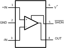
LMV601
DCK Package
DCK Package
6-Pin SC70
Top View

Pin Functions: LMV601
| PIN | I/O | DESCRIPTION | |
|---|---|---|---|
| NAME | NO. | ||
| GND | 2 | P | Supply negative input |
| +IN | 1 | I | Noninverting input |
| –IN | 3 | I | Inverting input |
| OUT | 4 | O | Output |
| SHDN | 5 | I | Active low enable input |
| V+ | 6 | P | Positive supply input |
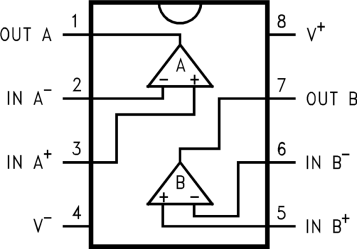
LMV602
DGK or D Packages
DGK or D Packages
8-Pin VSSOP or SOIC
Top View

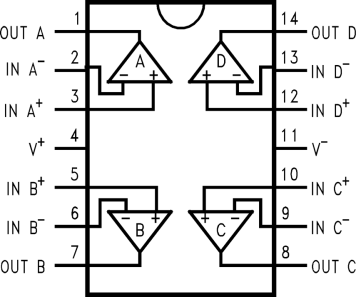
LMV604
PW or D Packages
PW or D Packages
14-Pin TSSOP and SOIC
Top View

Pin Functions: LMV602, LMV604
| PIN | I/O | DESCRIPTION | ||
|---|---|---|---|---|
| NAME | NO. | |||
| LMV602 | LMV604 | |||
| +INA | 3 | 3 | I | Noninverting input, channel A |
| +INB | 5 | 5 | I | Noninverting input, channel B |
| +INC | — | 10 | I | Noninverting input, channel C |
| +IND | — | 12 | I | Noninverting input, channel D |
| –INA | 2 | 2 | I | Inverting input, channel A |
| –INB | 6 | 6 | I | Inverting input, channel B |
| –INC | — | 9 | I | Inverting input, channel C |
| –IND | — | 13 | I | Inverting input, channel D |
| OUTA | 1 | 1 | O | Output, channel A |
| OUTB | 7 | 7 | O | Output, channel B |
| OUTC | — | 8 | O | Output, channel C |
| OUTD | — | 14 | O | Output, channel D |
| V+ | 8 | 4 | P | Positive (highest) power supply |
| V– | 4 | 11 | P | Negative (lowest) power supply |