SNOSC69D April 2012 – March 2017 LMV611 , LMV612 , LMV614
PRODUCTION DATA.
- 1 Features
- 2 Applications
- 3 Description
- 4 Revision History
- 5 Pin Configuration and Functions
-
6 Specifications
- 6.1 Absolute Maximum Ratings
- 6.2 ESD Ratings
- 6.3 Recommended Operating Conditions
- 6.4 Thermal Information
- 6.5 Electrical Characteristics - 1.8 V (DC)
- 6.6 Electrical Characteristics - 1.8 V (AC)
- 6.7 Electrical Characteristics - 2.7 V (DC)
- 6.8 Electrical Characteristics - 2.7 V (AC)
- 6.9 Electrical Characteristics - 5 V (DC)
- 6.10 Electrical Characteristics - 5 V (AC)
- 6.11 Typical Characteristics
- 7 Detailed Description
- 8 Application and Implementation
- 9 Power Supply Recommendations
- 10Layout
- 11Device and Documentation Support
- 12Mechanical, Packaging, and Orderable Information
パッケージ・オプション
メカニカル・データ(パッケージ|ピン)
サーマルパッド・メカニカル・データ
発注情報
7 Detailed Description
7.1 Overview
The LMV61x devices achieve a gain bandwidth of 1.4 MHz while drawing 100-µA (typical) quiescent current. They also provide a rail-to-rail input with a maximum input offset voltage of 4 mV. Lastly, the LMV61x input common mode extends 200 mV beyond the supplies and the output can swing rail-to-rail unloaded and within
30 mV with 2-kΩ load at 1.8-V supply.
7.2 Functional Block Diagram

7.3 Feature Description
7.3.1 Input and Output Stage
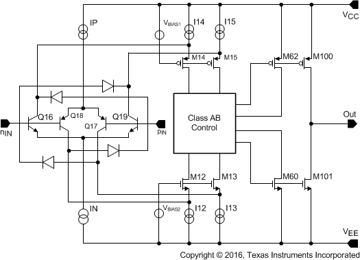
The rail-to-rail input stage of this family provides more flexibility for the designer. The LMV61x use a complimentary PNP and NPN input stage in which the PNP stage senses common-mode voltage near V− and the NPN stage senses common-mode voltage near V+. The transition from the PNP stage to NPN stage occurs
1 V below V+. Because both input stages have their own offset voltage, the offset of the amplifier becomes a function of the input common-mode voltage and has a crossover point at 1 V below V+.
This VOS crossover point can create problems for both DC- and AC-coupled signals if proper care is not taken. Large input signals that include the VOS crossover point causes distortion in the output signal. One way to avoid such distortion is to keep the signal away from the crossover. For example, in a unity-gain buffer configuration and with VS = 5 V, a 5-V peak-to-peak signal contains input-crossover distortion while a 3-V peak-to-peak signal centered at 1.5 V does not contain input-crossover distortion as it avoids the crossover point. Another way to avoid large signal distortion is to use a gain of −1 circuit which avoids any voltage excursions at the input terminals of the amplifier. In that circuit, the common-mode DC voltage can be set at a level away from the VOS crossover point. For small signals, this transition in VOS shows up as a VCM dependent spurious signal in series with the input signal and can effectively degrade small signal parameters such as gain and common-mode rejection ratio. To resolve this problem, the small signal must be placed such that it avoids the VOS crossover point. In addition to the rail-to-rail performance, the output stage can provide enough output current to
drive 600-Ω loads. Because of the high current capability, take care to not exceed the 150°C maximum junction temperature specification.
7.4 Device Functional Modes
7.4.1 Input Bias Current Consideration
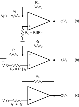
The LMV61x family has a complementary bipolar input stage. The typical input bias current (IB) is 15 nA. The input bias current can develop a significant offset voltage. This offset is primarily due to IB flowing through the negative feedback resistor, RF. For example, if IB is 50 nA and RF is 100 kΩ, then an offset voltage of 5 mV develops (VOS = IB × RF). Using a compensation resistor (RC), as shown in Figure 29, cancels this effect. But the input offset current (IOS) still contributes to an offset voltage in the same manner.
 Figure 29. Canceling Offset Voltage Due to Input Bias Current