SNOSC69D April 2012 – March 2017 LMV611 , LMV612 , LMV614
PRODUCTION DATA.
- 1 Features
- 2 Applications
- 3 Description
- 4 Revision History
- 5 Pin Configuration and Functions
-
6 Specifications
- 6.1 Absolute Maximum Ratings
- 6.2 ESD Ratings
- 6.3 Recommended Operating Conditions
- 6.4 Thermal Information
- 6.5 Electrical Characteristics - 1.8 V (DC)
- 6.6 Electrical Characteristics - 1.8 V (AC)
- 6.7 Electrical Characteristics - 2.7 V (DC)
- 6.8 Electrical Characteristics - 2.7 V (AC)
- 6.9 Electrical Characteristics - 5 V (DC)
- 6.10 Electrical Characteristics - 5 V (AC)
- 6.11 Typical Characteristics
- 7 Detailed Description
- 8 Application and Implementation
- 9 Power Supply Recommendations
- 10Layout
- 11Device and Documentation Support
- 12Mechanical, Packaging, and Orderable Information
パッケージ・オプション
メカニカル・データ(パッケージ|ピン)
サーマルパッド・メカニカル・データ
発注情報
10 Layout
10.1 Layout Guidelines
To properly bypass the power supply, several locations on a printed-circuit board must be considered. A
6.8-µF or greater tantalum capacitor must be placed at the point where the power supply for the amplifier is introduced onto the board. Another 0.1-µF ceramic capacitor must be placed as close as possible to the power supply pin of the amplifier. If the amplifier is operated in a single power supply, only the V+ pin must be bypassed with a 0.1-µF capacitor. If the amplifier is operated in a dual power supply, both V+ and V– pins must be bypassed.
It is good practice to use a ground plane on a printed-circuit board to provide all components with a low inductive ground connection.
TI recommends surface-mount components in 0805 size or smaller in the LMV611-N application circuits. Designers can take advantage of the VSSOP miniature sizes to condense board layout to save space and reduce stray capacitance.
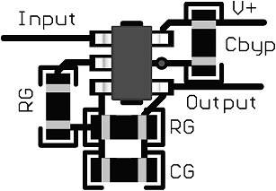
10.2 Layout Example
 Figure 35. SOT-23 Layout Example