JAJSDL5 May   2017 LMV931-N-Q1 , LMV932-N-Q1 , LMV934-N-Q1

PRODUCTION DATA.  

  1. 特長
  2. アプリケーション
  3. 概要
  4. 改訂履歴
  5. Pin Configuration and Functions
  6. Specifications
    1. 6.1  Absolute Maximum Ratings
    2. 6.2  ESD Ratings
    3. 6.3  Recommended Operating Ratings
    4. 6.4  Thermal Information
    5. 6.5  DC Electrical Characteristics 1.8 V
    6. 6.6  AC Electrical Characteristics 1.8 V
    7. 6.7  DC Electrical Characteristics 2.7 V
    8. 6.8  AC Electrical Characteristics 2.7 V
    9. 6.9  Electrical Characteristics 5 V DC
    10. 6.10 AC Electrical Characteristics 5 V
    11. 6.11 Typical Characteristics
  7. Detailed Description
    1. 7.1 Overview
    2. 7.2 Functional Block Diagram
    3. 7.3 Feature Description
    4. 7.4 Device Functional Modes
      1. 7.4.1 Input and Output Stage
      2. 7.4.2 Input Bias Current Consideration
  8. Application and Implementation
    1. 8.1 Application Information
    2. 8.2 Typical Applications
      1. 8.2.1 High-Side Current-Sensing Application
        1. 8.2.1.1 Design Requirements
          1. 8.2.1.1.1 Custom Design With WEBENCH® Tools
        2. 8.2.1.2 Detailed Design Procedure
        3. 8.2.1.3 Application Curve
      2. 8.2.2 Half-Wave Rectifier Applications
        1. 8.2.2.1 Design Requirements
        2. 8.2.2.2 Detailed Design Procedure
        3. 8.2.2.3 Application Curve
      3. 8.2.3 Instrumentation Amplifier With Rail-to-Rail Input and Output Application
        1. 8.2.3.1 Design Requirements
        2. 8.2.3.2 Detailed Design Procedure
        3. 8.2.3.3 Application Curve
    3. 8.3 Dos and Don'ts
  9. Power Supply Recommendations
  10. 10Layout
    1. 10.1 Layout Guidelines
    2. 10.2 Layout Example
  11. 11デバイスおよびドキュメントのサポート
    1. 11.1 デバイス・サポート
      1. 11.1.1 WEBENCH®ツールによるカスタム設計
      2. 11.1.2 開発サポート
    2. 11.2 ドキュメントのサポート
      1. 11.2.1 関連資料
    3. 11.3 関連リンク
    4. 11.4 ドキュメントの更新通知を受け取る方法
    5. 11.5 コミュニティ・リソース
    6. 11.6 商標
    7. 11.7 静電気放電に関する注意事項
    8. 11.8 Glossary
  12. 12メカニカル、パッケージ、および注文情報

パッケージ・オプション

メカニカル・データ(パッケージ|ピン)
サーマルパッド・メカニカル・データ
発注情報

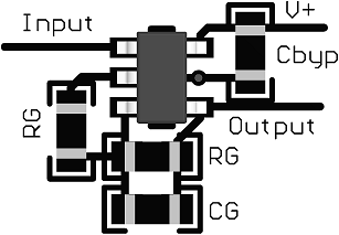
Layout

Layout Guidelines

The V+ pin must be bypassed to ground with a low-ESR capacitor.

The optimum placement is closest to the V+ and ground pins.

Take care to minimize the loop area formed by the bypass capacitor connection between V+ and ground.

The ground pin must be connected to the PCB ground plane at the pin of the device.

The feedback components should be placed as close as possible to the device minimizing strays.

Layout Example

LMV931-N-Q1 LMV932-N-Q1 LMV934-N-Q1 Layout_3D.png Figure 39. SOT-23 Layout Example