SNOSAI3D October   2006  – September 2015 LMV951

PRODUCTION DATA.  

  1. Features
  2. Applications
  3. Description
  4. Revision History
  5. Pin Configuration and Functions
  6. Specifications
    1. 6.1 Absolute Maximum Ratings
    2. 6.2 ESD Ratings
    3. 6.3 Recommended Operating Conditions
    4. 6.4 Thermal Information
    5. 6.5 Electrical Characteristics: 1 V
    6. 6.6 Electrical Characteristics: 1.8 V
    7. 6.7 Typical Characteristics
  7. Detailed Description
    1. 7.1 Overview
    2. 7.2 Functional Block Diagram
    3. 7.3 Feature Description
      1. 7.3.1 Battery Operated Systems
      2. 7.3.2 Small Size
    4. 7.4 Device Functional Modes
      1. 7.4.1 Shutdown Capability
      2. 7.4.2 Rail-to-Rail Input
      3. 7.4.3 Rail-to-Rail Output
      4. 7.4.4 Driving Capacitive Load
  8. Application and Implementation
    1. 8.1 Application Information
    2. 8.2 Typical Applications
      1. 8.2.1 Two Wire Line Transmission
        1. 8.2.1.1 Design Requirements
        2. 8.2.1.2 Detailed Design Procedure
        3. 8.2.1.3 Application Curves
      2. 8.2.2 Bridge Configuration Amplifier
      3. 8.2.3 Virtual Ground Circuit
  9. Power Supply Recommendations
  10. 10Layout
    1. 10.1 Layout Guidelines
    2. 10.2 Layout Example
  11. 11Device and Documentation Support
    1. 11.1 Device Support
      1. 11.1.1 Development Support
    2. 11.2 Documentation Support
      1. 11.2.1 Related Documentation
    3. 11.3 Community Resources
    4. 11.4 Trademarks
    5. 11.5 Electrostatic Discharge Caution
    6. 11.6 Glossary
  12. 12Mechanical, Packaging, and Orderable Information

パッケージ・オプション

メカニカル・データ(パッケージ|ピン)
サーマルパッド・メカニカル・データ
発注情報

1 Features

  • (Typical 1-V Supply, Unless Otherwise Noted)
  • Ensured 1-V, 380-µA Single-Supply Operation
  • Shutdown to 50-nA Supply Current
  • Wide 2.7-MHz Bandwidth
  • Rail-to-Rail Input With Zero Crossover
  • No Input IBIAS Current Reversal Over VCM Range
  • 1000-pF Output Drive Capability
  • High-Output Drive Capability
    • Sink Current: 35 mA
    • Source Current: 45 mA
  • Rail-to-Rail Buffered Output
    • At 600-Ω Load, 32 mV from Either Rail
    • At 2-kΩ Load, 12 mV from Either Rail
  • Temperature Range −40°C to 125°C

2 Applications

  • Battery Operated Systems
  • Battery Monitoring
  • Supply Current Monitoring

3 Description

The LMV951 amplifier is capable of operating at supply voltages from 0.9 V to 3 V with specified specs at 1-V and 1.8-V single supply.

The input common-mode range extends to both power supply rails without the offset transition zone and input bias current reversal inherent to most rail-to-rail input amplifiers.

Contrary to a conventional rail-to-rail output amplifier, the LMV951 has a buffered output stage, providing an open-loop gain which is relatively unaffected by resistive output loading. At 1-V supply voltage, the LMV951 is able to source and sink in excess of
35 mA and offers a gain bandwidth product of
2.7 MHz.

In shutdown mode, the LMV951 consumes less than 50 nA of supply current.

Device Information(1)

PART NUMBER PACKAGE BODY SIZE (NOM)
LMV951 SOT (6) 2.90 mm × 1.60 mm
  1. For all available packages, see the orderable addendum at the end of the data sheet.

space

space

Simplified Schematic
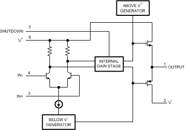
LMV951 20123104.gif

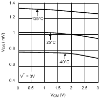
Offset Voltage Change vs Common Mode

LMV951 20123112.gif