SNAS187D February   2003  – January 2016 LMX2430 , LMX2433 , LMX2434

PRODUCTION DATA.  

  1. Features
  2. Applications
  3. Description
  4. Revision History
  5. Description continued
  6. Pin Configuration and Functions
  7. Specifications
    1. 7.1 Absolute Maximum Ratings
    2. 7.2 Recommended Operating Conditions
    3. 7.3 Thermal Information
    4. 7.4 Electrical Characteristics
    5. 7.5 Timing Requirements
    6. 7.6 Typical Characteristics
      1. 7.6.1 Sensitivity
      2. 7.6.2 Charge Pump
      3. 7.6.3 Input Impedance
  8. Parameter Measurement Information
    1. 8.1 Bench Test Setups
      1. 8.1.1 LMX243x Charge-Pump Test Setup
      2. 8.1.2 Charge-Pump Current Specification Definitions
        1. 8.1.2.1 Charge-Pump Output Current Variation vs Charge-Pump Output Voltage
        2. 8.1.2.2 Charge-Pump Sink Current vs Charge-Pump Output Source Current Mismatch
        3. 8.1.2.3 Charge-Pump Output Current Variation vs Temperature
      3. 8.1.3 LMX243x FinRF Sensitivity Test Setup
      4. 8.1.4 LMX243x OSCin Sensitivity Test Setup
      5. 8.1.5 LMX243x FinRF Input Impedance Test Setup
  9. Detailed Description
    1. 9.1 Overview
    2. 9.2 Functional Block Diagram
    3. 9.3 Feature Description
      1. 9.3.1  Reference Oscillator Input
      2. 9.3.2  Reference Dividers (R Counters)
      3. 9.3.3  Prescalers
      4. 9.3.4  Programmable Feedback Dividers (N Counters)
      5. 9.3.5  Phase / Frequency Detectors
        1. 9.3.5.1 Phase Comparator and Internal Charge-Pump Characteristics
      6. 9.3.6  Charge Pumps
      7. 9.3.7  Microwire Serial Interface
      8. 9.3.8  Multi-Function Outputs
        1. 9.3.8.1 Push-Pull Analog Lock-Detect Output
        2. 9.3.8.2 Open-Drain Analog Lock-Detect Output
        3. 9.3.8.3 Digital Filtered Lock-Detect Output
        4. 9.3.8.4 Reference Divider and Feedback Divider Output
      9. 9.3.9  Fastlock Output
      10. 9.3.10 Counter Reset
    4. 9.4 Device Functional Modes
      1. 9.4.1 Power Control
        1. 9.4.1.1 Synchronous Power-Down Mode
        2. 9.4.1.2 Asynchronous Power-Down Mode
    5. 9.5 Programming
      1. 9.5.1 Microwire Interface
      2. 9.5.2 Control Register Location
    6. 9.6 Register Maps
      1. 9.6.1 Control Register Content Map
      2. 9.6.2 R0 Register
        1. 9.6.2.1 RF_R[14:0] - RF Synthesizer Programmable Reference Divider (R Counter) (R0[17:3])
        2. 9.6.2.2 RF_CPP - RF Synthesizer Phase Detector Polarity (R0[18])
        3. 9.6.2.3 RF_CPG - RF Synthesizer Charge-Pump Current Gain (R0[19])
        4. 9.6.2.4 RF_CPT - RF Synthesizer Charge-Pump Tri-State (R0[20])
        5. 9.6.2.5 RF_RST - RF Synthesizer Counter Reset (R0[21])
      3. 9.6.3 R1 Register
        1. 9.6.3.1 LMX243x RF Synthesizer Swallow Counter
          1. 9.6.3.1.1 RF_A[3:0] - LMX2430/33 RF Synthesizer Swallow Counter (A Counter) (R1[6:3])
          2. 9.6.3.1.2 RF_A[4:0] - LMX2434 RF Synthesizer Swallow Counter (A Counter) (R1[7:3])
        2. 9.6.3.2 LMX243x RF Synthesizer Programmable Binary Counter
          1. 9.6.3.2.1 RF_B[14:0] - LMX2430/33 RF Synthesizer Programmable Binary Counter (B Counter) (R1[21:7])
          2. 9.6.3.2.2 RF_B[13:0] - LMX2434 RF Synthesizer Programmable Binary Counter (B Counter) (R1[21:8])
        3. 9.6.3.3 LMX243x RF Synthesizer Prescaler Select
          1. 9.6.3.3.1 RF_P - LMX2430/33 RF Synthesizer Prescaler Select (R1[22])
          2. 9.6.3.3.2 RF_P - LMX2434 RF Synthesizer Prescaler Select (R1[22])
        4. 9.6.3.4 RF_PD - RF Synthesizer Power Down (R1[23])
      4. 9.6.4 R2 Register
        1. 9.6.4.1 RF_TOC[0:11] - RF Synthesizer Time-Out Counter (R2[14:3])
        2. 9.6.4.2 R3 Register
          1. 9.6.4.2.1 IF_R[14:0] - IF Synthesizer Programmable Reference Divider (R Counter) (R3[17:3])
          2. 9.6.4.2.2 IF_CPP - IF Synthesizer Phase Detector Polarity (R3[18])
          3. 9.6.4.2.3 IF_CPG - IF Synthesizer Charge-Pump Current Gain (R3[19])
          4. 9.6.4.2.4 IF_CPT - IF Synthesizer Charge-Pump Tri-State (R3[20])
          5. 9.6.4.2.5 IF_RST - IF Synthesizer Counter Reset (R3[21])
      5. 9.6.5 R4 Register
        1. 9.6.5.1 IF_A[3:0] - IF Synthesizer Swallow Counter (A Counter) (R4[6:3])
        2. 9.6.5.2 IF_B[13:0] - IF Synthesizer Programmable Binary Counter (B Counter) (R4[20:7])
          1. 9.6.5.2.1 IF_P - IF Synthesizer Prescaler Select (R4[22])
        3. 9.6.5.3 IF_PD - IF Synthesizer Power Down (R4[23])
      6. 9.6.6 R5 Register
        1. 9.6.6.1 IF_TOC[0:11] - IF Synthesizer Time-Out Counter (R5[14:3])
      7. 9.6.7 MUX[3:0] - Multifunction Output Select (R3[23:22]:R0[23:22])
  10. 10Application and Implementation
    1. 10.1 Application Information
    2. 10.2 Typical Application
      1. 10.2.1 Design Requirements
      2. 10.2.2 Detailed Design Procedure
      3. 10.2.3 Application Curves
  11. 11Power Supply Recommendations
  12. 12Layout
    1. 12.1 Layout Guidelines
    2. 12.2 Layout Example
  13. 13Device and Documentation Support
    1. 13.1 Device Support
      1. 13.1.1 Device Nomenclature
        1. 13.1.1.1 List of Definitions
    2. 13.2 Related Links
    3. 13.3 Community Resources
    4. 13.4 Trademarks
    5. 13.5 Electrostatic Discharge Caution
    6. 13.6 Glossary
  14. 14Mechanical, Packaging, and Orderable Information

パッケージ・オプション

メカニカル・データ(パッケージ|ピン)
サーマルパッド・メカニカル・データ
発注情報

12 Layout

12.1 Layout Guidelines

In general, there are two cases for layout:

  1. Use as a single PLL: In this case, all power supply pins must be connected, but for those on the unused PLL, bypassing is not necessary, and they can be shorted together. Leave unused outputs unconnected, and do not ground them.
  2. Use as a dual PLL: In this case, supply coupling is much more critical as there can be crosstalk between the two PLLs. There must be isolation in the form of resistors or inductors between the charge-pump supply pins, and decoupling capacitors are more important.

12.2 Layout Example
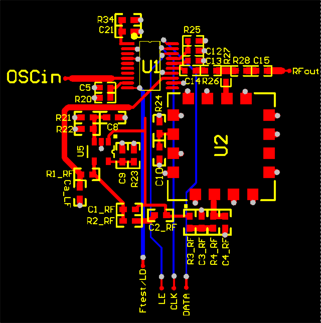
LMX2430 LMX2433 LMX2434 pcb_snas187.gif Figure 36. Layout Example