JAJSCK2A October 2016 – January 2017 LMX2491
PRODUCTION DATA.
- 1 特長
- 2 アプリケーション
- 3 概要
- 4 改訂履歴
- 5 Pin Configuration and Functions
- 6 Specifications
-
7 Detailed Description
- 7.1 Overview
- 7.2 Functional Block Diagram
- 7.3
Feature Description
- 7.3.1 OSCin Input
- 7.3.2 OSCin Doubler
- 7.3.3 R Divider
- 7.3.4 PLL N Divider
- 7.3.5 Fractional Circuitry
- 7.3.6 PLL Phase Detector and Charge Pump
- 7.3.7 External Loop Filter
- 7.3.8 Fastlock and Cycle Slip Reduction
- 7.3.9 Lock Detect and Charge Pump Voltage Monitor
- 7.3.10 FSK/PSK Modulation
- 7.3.11 Ramping Functions
- 7.3.12 Power-on-reset (POR)
- 7.3.13 Register Readback
- 7.4 Device Functional Modes
- 7.5 Programming
- 7.6 Register Maps
-
8 Applications and Implementation
- 8.1 Application Information
- 8.2
Typical Application
- 8.2.1 Design Requirements
- 8.2.2 Detailed Design Procedure
- 8.2.3 TICS Pro Basic Setup
- 8.2.4 Frequency Shift Keying Example
- 8.2.5 Single Sawtooth Ramp Example
- 8.2.6 Continuous Sawtooth Ramp Example
- 8.2.7 Continuous Sawtooth Ramp with FSK Example
- 8.2.8 Continuous Triangular Ramp Example
- 8.2.9 Continuous Trapezoid Ramp Example
- 8.2.10 Arbitrary Waveform Ramp Example
- 9 Power Supply Recommendations
- 10Layout
- 11デバイスおよびドキュメントのサポート
- 12メカニカル、パッケージ、および注文情報
パッケージ・オプション
メカニカル・データ(パッケージ|ピン)
- RTW|24
サーマルパッド・メカニカル・データ
- RTW|24
発注情報
10 Layout
10.1 Layout Guidelines
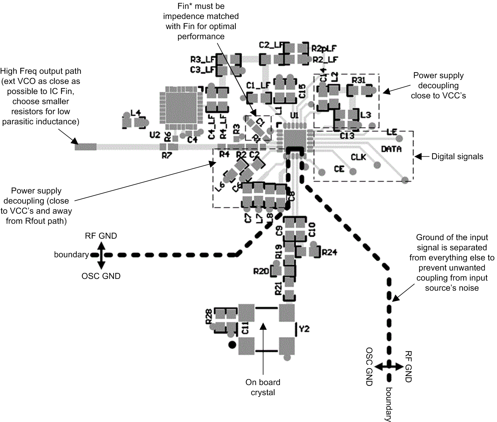
For layout examples, the EVM instructions are the most comprehensive document. In general, the layout guidelines are similar to most other PLL devices. For the high frequency Fin pin, it is recommended to use 0402 components and match the trace width to these pad sizes. Also the same needs to be done on the Fin* pin. If layout is easier to route the signal to Fin* instead of Fin, then this is acceptable as well.
10.2 Layout Example
 Figure 33. Layout Recommendation