JAJSCK2A October 2016 – January 2017 LMX2491
PRODUCTION DATA.
- 1 特長
- 2 アプリケーション
- 3 概要
- 4 改訂履歴
- 5 Pin Configuration and Functions
- 6 Specifications
-
7 Detailed Description
- 7.1 Overview
- 7.2 Functional Block Diagram
- 7.3
Feature Description
- 7.3.1 OSCin Input
- 7.3.2 OSCin Doubler
- 7.3.3 R Divider
- 7.3.4 PLL N Divider
- 7.3.5 Fractional Circuitry
- 7.3.6 PLL Phase Detector and Charge Pump
- 7.3.7 External Loop Filter
- 7.3.8 Fastlock and Cycle Slip Reduction
- 7.3.9 Lock Detect and Charge Pump Voltage Monitor
- 7.3.10 FSK/PSK Modulation
- 7.3.11 Ramping Functions
- 7.3.12 Power-on-reset (POR)
- 7.3.13 Register Readback
- 7.4 Device Functional Modes
- 7.5 Programming
- 7.6 Register Maps
-
8 Applications and Implementation
- 8.1 Application Information
- 8.2
Typical Application
- 8.2.1 Design Requirements
- 8.2.2 Detailed Design Procedure
- 8.2.3 TICS Pro Basic Setup
- 8.2.4 Frequency Shift Keying Example
- 8.2.5 Single Sawtooth Ramp Example
- 8.2.6 Continuous Sawtooth Ramp Example
- 8.2.7 Continuous Sawtooth Ramp with FSK Example
- 8.2.8 Continuous Triangular Ramp Example
- 8.2.9 Continuous Trapezoid Ramp Example
- 8.2.10 Arbitrary Waveform Ramp Example
- 9 Power Supply Recommendations
- 10Layout
- 11デバイスおよびドキュメントのサポート
- 12メカニカル、パッケージ、および注文情報
パッケージ・オプション
メカニカル・データ(パッケージ|ピン)
- RTW|24
サーマルパッド・メカニカル・データ
- RTW|24
発注情報
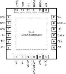
5 Pin Configuration and Functions
RTW Package
24-Pin VQFN
Top View

Pin Functions
| TERMINAL | TYPE | DESCRIPTION | |
|---|---|---|---|
| NO. | NAME | ||
| 0 | DAP | GND | Die Attach Pad. Connect to PCB ground plane. |
| 1 | GND | GND | Ground for charge pump. |
| 2, 3 | GND | GND | Ground for Fin Buffer |
| 4, 5 | Fin Fin* |
Input | Complimentary high frequency input pins. Should be AC-coupled. If driving single-ended, impedance as seen from Fin and Fin* pins looking outwards from the part should be roughly the same. |
| 6 | Vcc | Supply | Power Supply for Fin Buffer |
| 7 | Vcc | Supply | Supply for On-chip LDOs |
| 8 | Vcc | Supply | Supply for OSCin Buffer |
| 9 | OSCin | Input | Reference Frequency Input |
| 10 | GND/ OSCin* |
GND/Input | Complimentary input for OSCin. If not used, it is recommended to match the termination as seen from the OSCin terminal looking outwards. However, this may also be grounded as well. |
| 11 | GND | GND | Ground for OSCin Buffer |
| 12 | MOD | Input/Output | Multiplexed Input/Output Pins for Ramp Triggers, FSK/PSK Modulation, FastLock, and Diagnostics |
| 13 | CE | Input | Chip Enable |
| 14 | CLK | GND | Serial Programming Clock. |
| 15 | DATA | GND | Serial Programming Data |
| 16 | LE | Input | Serial Programming Latch Enable |
| 17 | MUXout | Input/Output | Multiplexed Input/Output Pins for Ramp Triggers, FSK/PSK Modulation, FastLock, and Diagnostics |
| 18 | Vcc | Supply | Supply for delta sigma engine. |
| 19 | Vcc | Supply | Supply for general circuitry. |
| 20 | TRIG1 | Input/Output | Multiplexed Input/Output Pins for Ramp Triggers, FSK/PSK Modulation, FastLock, and Diagnostics |
| 21 | TRIG2 | Input/Output | Multiplexed Input/Output Pins for Ramp Triggers, FSK/PSK Modulation, FastLock, and Diagnostics |
| 22 | Vcp | Supply | Power Supply for the charge pump. |
| 23 | Rset | NC | No connect. |
| 24 | CPout | Output | Charge Pump Output |