6 Specifications
6.1 Absolute Maximum Ratings
over operating free-air temperature range (unless otherwise noted) (1)
|
MIN |
MAX |
UNIT |
| VCP |
Supply voltage for charge pump |
VCC |
5.5 |
V |
| VCC |
Supply voltage |
–0.3 |
3.6 |
V |
| VIN |
I/O input voltage |
–0.3 |
VCC + 0.3 |
V |
| TSolder |
Lead temperature (solder 4 seconds) |
|
260 |
°C |
| TJunction |
Junction temperature |
|
150 |
°C |
(1) Stresses beyond those listed under Absolute Maximum Ratings may cause permanent damage to the device. These are stress ratings only, which do not imply functional operation of the device at these or any other conditions beyond those indicated under Recommended Operating Conditions. Exposure to absolute-maximum-rated conditions for extended periods may affect device reliability.
6.2 Storage Conditions
applicable before the DMD is installed in the final product
|
MIN |
MAX |
UNIT |
| Tstg |
DMD storage temperature |
–65 |
150 |
°C |
| TDP |
Storage dew point |
|
3 |
°C |
6.3 ESD Ratings
|
VALUE |
UNIT |
| V(ESD) |
Electrostatic discharge |
Human-body model (HBM), per ANSI/ESDA/JEDEC JS-001(1) |
±2500 |
V |
| Charged-device model (CDM), per JEDEC specification JESD22-C101(2) |
±1500 |
(1) JEDEC document JEP155 states that 500-V HBM allows safe manufacturing with a standard ESD control process.
(2) JEDEC document JEP157 states that 250-V CDM allows safe manufacturing with a standard ESD control process.
6.4 Recommended Operating Conditions
over operating free-air temperature range (unless otherwise noted)
| PARAMETER |
MIN |
NOM |
MAX |
UNIT |
| VCC |
Supply voltage |
3.15 |
3.3 |
3.45 |
V |
| VCP |
Charge pump supply voltage |
VCC |
|
5.25 |
V |
| TA |
Ambient temperature |
–40 |
|
85 |
°C |
| TJ |
Junction temperature |
–40 |
|
125 |
°C |
6.5 Thermal Information
| THERMAL METRIC(1) |
LMX2491 |
UNIT |
| RTW (VQFN) |
| 24 PINS |
| RθJA |
Junction-to-ambient thermal resistance |
39.4 |
°C/W |
| RθJC(top) |
Junction-to-case (top) thermal resistance |
7.1 |
°C/W |
| ψJB |
Junction-to-board characterization parameter |
20 |
°C/W |
6.6 Electrical Characteristics
3.15 V ≤ VCC ≤ 3.45 V, VCC ≤ VCP ≤ 5.25 V, –40 °C ≤ TA ≤ 85 °C, except as specified. Typical values are at VCC = VCP = 3.3 V, 25 °C.
| PARAMETER |
TEST CONDITIONS |
MIN |
TYP |
MAX |
UNIT |
| ICC |
Current consumption |
All Vcc pins |
fPD = 10 MHz |
|
45 |
|
mA |
| fPD = 100 MHz |
|
50 |
|
| fPD = 200 MHz |
|
55 |
|
| Vcp pin |
KPD = 0.1 mA |
|
2 |
|
| KPD = 1.6 mA |
|
10 |
|
| KPD = 3.1 mA |
|
19 |
|
| ICCPD |
Power down current |
POWERDOWN |
|
3 |
|
| fOSCin |
Frequency for OSCin terminal |
OSC_DIFFR = 0, doubler disabled |
10 |
|
600 |
MHz |
| OSC_DIFFR = 0, doubler enabled |
10 |
|
300 |
| OSC_DIFFR = 1, doubler disabled |
10 |
|
1200 |
| OSC_DIFFR = 1, doubler enabled |
10 |
|
600 |
| VOSCin |
Voltage for OSCin pin(1) |
|
0.5 |
|
VCC – 0.5 |
VPP |
| fFin |
Frequency for Fin pin |
|
500 |
|
6400 |
MHz |
| PFin |
Power for Fin pin |
Single-ended operation |
–5 |
|
5 |
dBm |
| fPD |
Phase detector frequency |
|
|
|
200 |
MHz |
| PN1Hz |
PLL figure of merit(2) |
|
|
–227 |
|
dBc/Hz |
| PN10kHz |
Normalized PLL 1/f noise(2) |
Normalized to 10-kHz offset for a 1-GHz carrier. |
|
–120 |
|
dBc/Hz |
| ICPoutTRI |
Charge pump leakage tri-state leakage |
|
|
|
10 |
nA |
| ICPoutMM |
Charge pump mismatch(3) |
VCPout = VCP / 2 |
|
5% |
|
|
| ICPout |
Charge pump current |
VCPout = VCP / 2 |
CPG = 1X |
|
0.1 |
|
mA |
| … |
|
|
|
| CPG = 31X |
|
3.1 |
|
| LOGIC OUTPUT TERMINALS (MUXout, TRIG1, TRIG2, MOD) |
| VOH |
Output high voltage |
|
0.8 × VCC |
VCC |
|
V |
| VOL |
Output low voltage |
|
|
0 |
0.2 × VCC |
V |
| LOGIC INPUT TERMINALS (CE, CLK, DATA, LE, MUXout, TRIG1, TRIG2, MOD) |
| VIH |
Input high voltage |
|
1.4 |
|
VCC |
V |
| VIL |
Input low voltage |
|
0 |
|
0.6 |
V |
| IIH |
Input leakage current |
|
–5 |
1 |
5 |
µA |
| tCELOW |
Chip enable low time |
|
5 |
|
|
µs |
| tCEHIGH |
Chip enable high time |
|
5 |
|
|
µs |
(1) For optimal phase noise performance, higher input voltage and a slew rate of at least 3 V/ns is recommended
(2) PLL Noise Metrics are measured with a clean OSCin signal with a high slew rate using a wide loop bandwidth. The noise metrics model the PLL noise for an infinite loop bandwidth as:
PLL_Total = 10 × log( 10PLL_Flat / 10 + 10PLL_Flicker(Offset) / 10)
PLL_Flat = PN1Hz + 20 × log(N) + 10 × log(fPD / 1 Hz)
PLL_Flicker = PN10kHz - 10 × log(Offset / 10 kHz) + 20 × log(fVCO / 1 GHz)
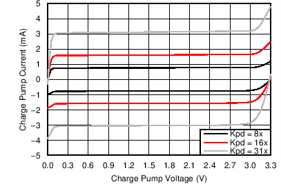
(3) Charge pump mismatch varies as a function of charge pump voltage. Consult typical performance characteristics to see this variation.
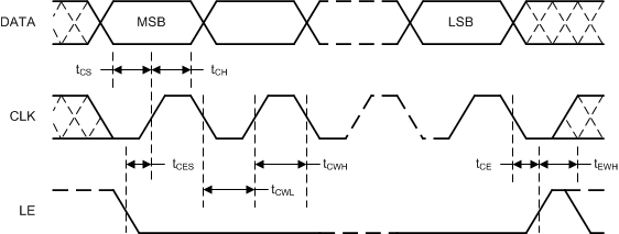
6.7 Timing Requirements, Programming Interface (CLK, DATA, LE)
| |
MIN |
TYP |
MAX |
UNIT |
| tCE |
Clock to LE low time |
10 |
|
|
ns |
| tCS |
Data to clock setup time |
4 |
|
|
ns |
| tCH |
Data to clock hold time |
4 |
|
|
ns |
| tCWH |
Clock pulse width high |
10 |
|
|
ns |
| tCWL |
Clock pulse width low |
10 |
|
|
ns |
| tCES |
Enable to clock setup time |
10 |
|
|
ns |
| tEWH |
Enable pulse width high |
10 |
|
|
ns |
There are several other considerations for programming:
- The DATA is clocked into a shift register on each rising edge of the CLK signal. On the rising edge of the LE signal, the data is sent from the shift register to an actual counter.
- If no LE signal is given after the last data bit and the clock is kept toggling, then these bits are read into the next lower register. This eliminates the need to send the address each time.
- A slew rate of at least 30 V/µs is recommended for the CLK, DATA, and LE signals
- Timing specs also apply to readback. Readback can be done through the MUXout, TRIG1, TRIG2, or MOD terminals.
6.8 Typical Characteristics

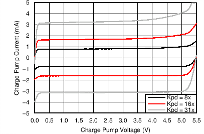
| Optimal performance is for a typical charge pump output voltage between 0.5 and 2.8 volts. |
Figure 2. Charge Pump Current for VCP = 3.3 V
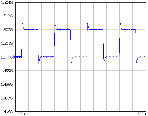
 Figure 4. Frequency Shift Keying
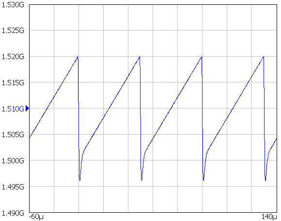
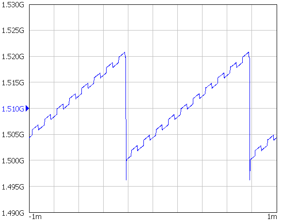
 Figure 6. Continuous Sawtooth Ramp
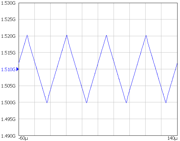
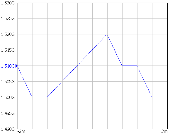
 Figure 8. Continuous Triangular Ramp
 Figure 10. Arbitrary Waveform Ramp

| Optimal performance is typically for a charge pump output voltage between 0.5 and 4.5 volts. |
Figure 3. Charge Pump Current for VCP = 5.5 V
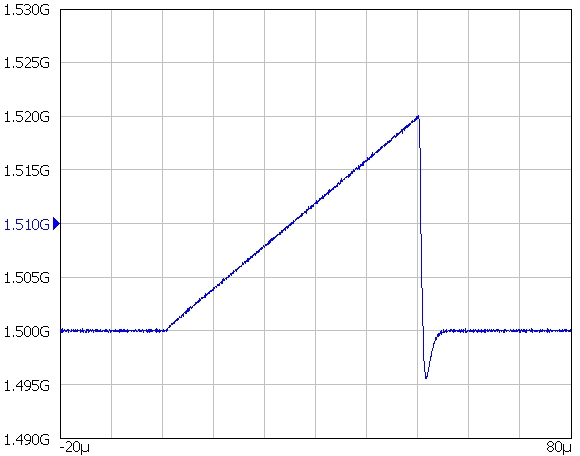
 Figure 5. Single Sawtooth Ramp
 Figure 7. Continuous Sawtooth Ramp with FSK
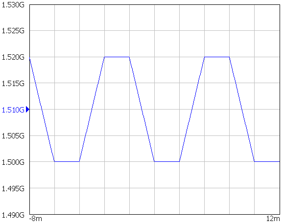
 Figure 9. Continuous Trapezoid Ramp
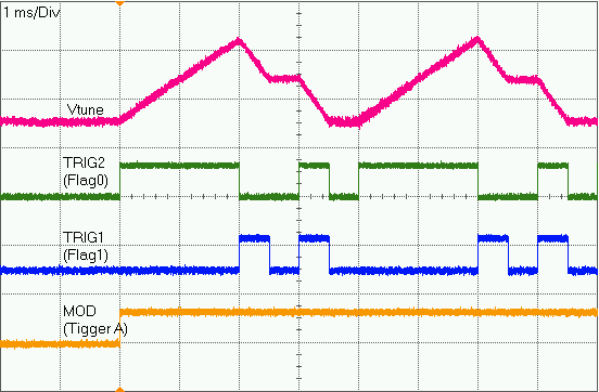
 Figure 11. Output Flags
