SNAS624B March 2014 – May 2015 LMX2492 , LMX2492-Q1
PRODUCTION DATA.
- 1 Features
- 2 Applications
- 3 Description
- 4 Simplified Schematic
- 5 Revision History
- 6 Pin Configuration and Functions
- 7 Specifications
-
8 Detailed Description
- 8.1 Overview
- 8.2 Functional Block Diagram
- 8.3
Feature Description
- 8.3.1 OSCin Input
- 8.3.2 OSCin Doubler
- 8.3.3 R Divider
- 8.3.4 PLL N Divider
- 8.3.5 Fractional Circuitry
- 8.3.6 PLL Phase Detector and Charge Pump
- 8.3.7 External Loop Filter
- 8.3.8 Fastlock and Cycle Slip Reduction
- 8.3.9 Lock Detect and Charge Pump Voltage Monitor
- 8.3.10 FSK/PSK Modulation
- 8.3.11 Ramping Functions
- 8.3.12 Power on Reset (POR)
- 8.4 Device Functional Modes
- 8.5 Programming
- 8.6 Register Map
- 8.7 Register Field Descriptions
- 8.8 Lock Detect and Charge Pump Monitoring
- 8.9 TRIG1,TRIG2,MOD, and MUXout Pins
- 8.10 Ramping Functions
- 8.11 Individual Ramp Controls
- 9 Applications and Implementation
- 10Power Supply Recommendations
- 11Layout
- 12Device and Documentation Support
- 13Mechanical, Packaging, and Orderable Information
パッケージ・オプション
メカニカル・データ(パッケージ|ピン)
- RTW|24
サーマルパッド・メカニカル・データ
- RTW|24
発注情報
9 Applications and Implementation
NOTE
Information in the following applications sections is not part of the TI component specification, and TI does not warrant its accuracy or completeness. TI’s customers are responsible for determining suitability of components for their purposes. Customers should validate and test their design implementation to confirm system functionality.
9.1 Application Information
The LMX2492/92-Q1 can be used in a broad class of applications such as generating a single frequency for a high frequency clock, generating a tunable range of frequencies, or generating swept waveforms that can be used in applications such as radar.
9.2 Typical Applications
The following schematic is an example of hat could be used in a typical application.
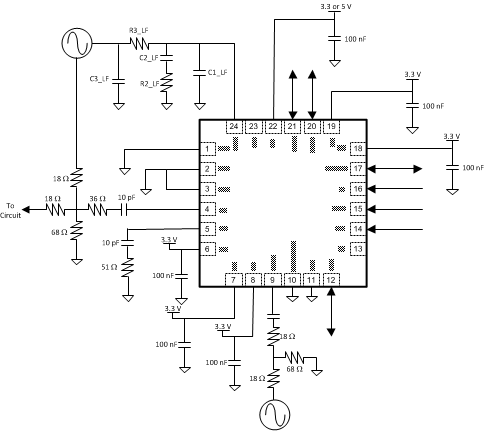
9.2.1 Design Requirements
For these examples, it will be assumed that there is a 100 MHz input signal and the output frequency is between 9400 and 9800 MHz with various modulated waveforms.
| Parameter | Symbol | Value | Comments |
|---|---|---|---|
| Input Frequency | OSCin | 100 MHz | |
| Phase Detector Frequency | Fpd | 100 MHz | There are many possibilities, but this choice gives good performance and saves a little current (as shown in the electrical specifications). |
| VCO Frequency | Fvco | 9400 - 9800 MHz (Simple Chirp) | In the different examples, the VCO frequency is actually changing. However, the same loop filter design can be used for all three. |
| 9400 - 9800 (Flattened Ramp) | |||
| 9500 - 9625 MHz (Complex Triggered Ramp | |||
| VCO Gain | Kvco | 200 MHz/V | This parameter has nothing to do with the LMX2492/92-Q1, but is rather set by the external VCO choice. |
9.2.2 Detailed Design Procedure
The first step is to calculate the reference divider (PLL_R) and feedback divider (PLL_N) values as shown in the table that follows.
| Parameter | Symbol and Calculations | Value | Comments |
|---|---|---|---|
| Average VCO Frequency |
FvcoAvg
= (FvcoMax + FvcoMin)/2 |
9600 MHz | To design a loop filter, one designs for a fixed VCO value, although it is understood that the VCO will tune around. This typical value is usually chosen as the average VCO frequency. |
| VCO Gain | Kvco | 200 MHz/V | This parameter has nothing to do with the LMX2492/92-Q1, but is rather set by the external VCO choice. In this case, it was the RFMD1843 VCO. |
| PLL Loop Bandwidth | BW | 380 kHz | This bandwidth is very wide to allow the VCO frequency to be modulated. |
| Charge Pump Gain | CPG | 3.1 mA | Using the larger gain allows a wider loop bandwidth and gives good phase performance. |
| R Divider | PLL_R = OSCin / Fpd |
1 | This value is calculated from previous values. |
| N Divider | PLL_N = Fvco / Fpd |
96 | This value is calculated from previous values. |
| Loop Filter Components | C1_LF | 68 pF | These were calculated by TI design tools. |
| C2_LF | 3.9 nF | ||
| C3_LF | 150 pF | ||
| R2_LF | 390 ohm | ||
| R3_LF | 390 ohm |
Once a loop filter bandwidth is chosen, the external loop filter components of C1_LF, C2_LF, C3_LF, R2_LF, and R3_LF can be calculated with a tool such as the Clock Architect tool available at www.ti.com. It is also highly recommended to look at the EVM instructions. The CodeLoader software is an excellent starting point and example to see how to program this device.
9.2.3 Application Performance Plot - Sawtooth Waveform Example
Using the above design, it can be programmed to generate a sawtooth waveform with the following paramters.
| Parameter | Symbol | Value |
|---|---|---|
| Ramp Duration | ΔT | 100 uS |
| VCO Frequency | Fvco | 9400 - 9800 MHz |
| Range | ΔF | 9400 - 9800 MHz = 400 MHz Change |
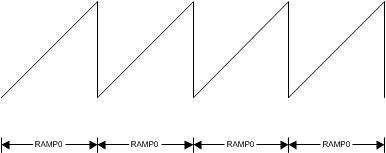
Because we want the ramp length to be 100 us, this works out to 10,000 phase detector cycles which means that RAMP0_LEN=10000. To change 400 MHz, we know that each one of the 10000 steps is 40 kHz. Given the fractional denominator is 224 = 16777216 and the phase detector frequency is 100 MHz, this implies that the fractional numerator at the end of the ramp will be 6711. However, since this 6711 number is not exact (closer to 6718.8864), the ramp will creep if we do not reset it. Therefore, we set reset the ramp. After the ramp finishes, we want to start with the same ramp, so RAMP0_NEXT is RAMP0. The results of this analysis are in the table below:
| RAMP | RAMP0_LEN | RAMP0_INC | RAMP0_NEXT | RAMP0_RST |
|---|---|---|---|---|
| RAMP0 | ΔT × Fpd = 100 us / 100 MHz = 10000 |
(ΔF / Fpd) /RAMP0_LEN × 224
= (400/100)/10000 ×16777216 = 6711 |
0 | 1 |
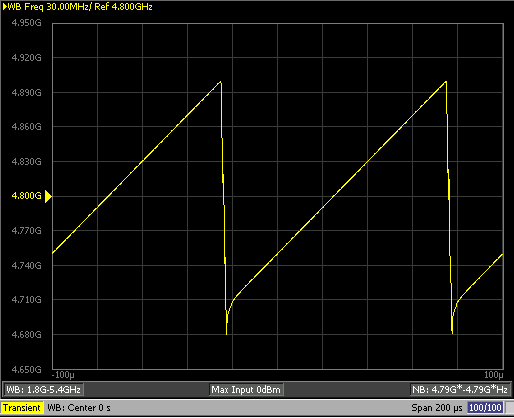
The actual measured waveform for this is shown in the following figure. Note that the frequency that was actually measured was from the divide by two output of the VCO and therefore the measured frequency was half of the actual frequency presented to the PLL. This ramping waveform does show some undershoot as the frequency rapidly returns from 9800 MHz ( 4900 MHz on the plot) to 9400 MHz (4700 MHz on the plot). This undershoot can be mitigated by adding additional ramps.
9.2.4 Application Performance Plot - Flat Top Triangle Waveform
Now consider pattern as shown below. The ramp is sometimes used because it can better account for Doppler Shift. The purpose for making the top and bottom portions flat is to help reduce the impact of the PLL overshooting and undershooting in order to make the sloped ramped portions more linear.
| Parameter | Symbol | Value |
|---|---|---|
| Ramp Duration | ΔT0 | 10 uS |
| ΔT1 | 90 uS | |
| ΔT2 | 10 uS | |
| ΔT3 | 90 uS | |
| Range | ΔF0 | 0 |
| ΔF1 | 400 MHz | |
| ΔF2 | 0 | |
| ΔF3 | -400 MHz |
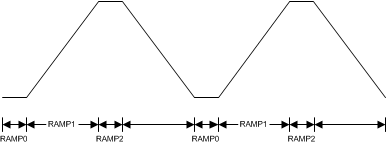
| RAMP | RAMPx_LEN | RAMPx_INC | RAMPx_NEXT | RAMPx_RST |
|---|---|---|---|---|
| RAMP0 | 10 us/ 100 MHz =1000 |
0 | 1 | 1 |
| RAMP1 | 90 us / 100 MHz =9000 |
(ΔF / Fpd) /RAMP1_LEN × 224
= (400/100)/9000 ×16777216 = 7457 |
2 | 0 |
| RAMP2 | 10 us/ 100 MHz =1000 |
0 | 3 | 0 |
| RAMP3 | 90 us / 100 MHz =9000 |
(ΔF / Fpd) /RAMP1_LEN × 224
= (-400/100)/9000 ×16777216 = -7457 Program in 2's complement of -7457 = 230-7457 = 1073734367 |
0 | 0 |
The actual measured waveform for this is shown in the following figure. Note that the frequency that was actually measured was from the divide by two output of the VCO and therefore the measured frequency was half of the actual frequency presented to the PLL. The flattened top and bottom of this triangle wave help mitigate the overshoot and undersoot in the frequency.
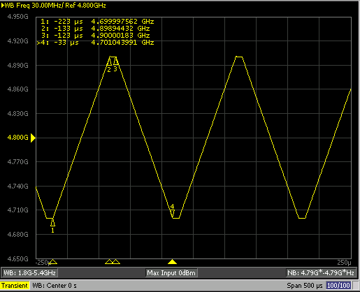
The actual measured waveform for this is shown in the following figure. Note that the frequency that was actually measured was from the divide by two output of the VCO and therefore the measured frequency was half of the actual frequency presented to the PLL. The flattened top and bottom of this triangle wave help mitigate the overshoot and undersoot in the frequency.
9.2.5 Applications Performance Plot -- Complex Triggered Ramp
In this example, the modulation is not started until a trigger pulse from the MOD terminal goes high. Assume a phase detector frequency of 100 MHz and we RAMP1 to be 60 us and ramps 2,3,and 4 to be 12 us each. We set the next trigger for RAMP0 to be trigger A and define trigger A to be the MOD terminal. Then we configure as follows:
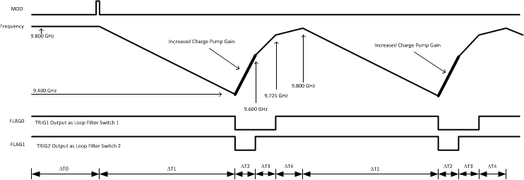 Figure 6. Complex Triggered Ramp Example
| RAMP | RAMPx _LEN |
RAMPx_ INC |
RAMPx_FL | RAMPx _NEXT |
RAMPx_FLAG | RAMPx_ NEXT_TRIG |
RAMPx_RST |
|---|---|---|---|---|---|---|---|
| RAMP0 | 1 | 0 | 0 | 1 | FLAG0 and FLAG1 | TRIG A | 1 |
| RAMP1 | 6000 | 1073730639 | 0 | 2 | FLAG0 and FLAG1 | TOC Timeout | 1 |
| RAMP2 | 1200 | 27963 | 1 | 3 | Disabled | TOC Timeout | 0 |
| RAMP3 | 1200 | 17476 | 0 | 4 | FLAG1 | TOC Timeout | 0 |
| RAMP4 | 1200 | 10486 | 0 | 1 | FLAG0 and FLAG1 | TOC Timeout | 0 |
The actual measured waveform for this is shown in the following figure. Note that the frequency that was actually measured was from the divide by two output of the VCO and therefore the measured frequency was half of the actual frequency presented to the PLL. The flattened top and bottom of this triangle wave help mitigate the overshoot and undersoot in the frequency.
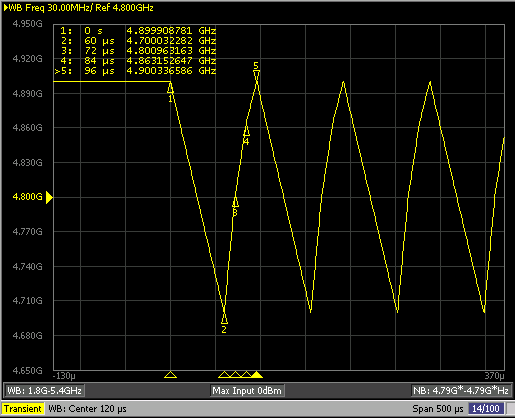 Figure 7. Actual Measurement for Complex Triggered Ramp