SNAS252S October 2005 – December 2014 LMX2531
PRODUCTION DATA.
- 1 Features
- 2 Applications
- 3 Description
- 4 Revision History
- 5 Pin Configuration and Functions
- 6 Specifications
-
7 Detailed Description
- 7.1 Overview
- 7.2 Functional Block Diagram
- 7.3 Feature Description
- 7.4 Device Functional Modes
- 7.5 Programming
- 7.6
Register Maps
- 7.6.1
General Programming Information
- 7.6.1.1 Initialization Sequence
- 7.6.1.2 Complete Register Content Map
- 7.6.1.3 Register R0
- 7.6.1.4 Register R1
- 7.6.1.5 Register R2
- 7.6.1.6 Register R3
- 7.6.1.7 Register R4
- 7.6.1.8
Register R5
- 7.6.1.8.1 EN_PLL -- Enable Bit for PLL
- 7.6.1.8.2 EN_VCO -- Enable Bit for the VCO
- 7.6.1.8.3 EN_OSC -- Enable Bit for the Oscillator Inverter
- 7.6.1.8.4 EN_VCOLDO -- Enable Bit for the VCO LDO
- 7.6.1.8.5 EN_PLLLDO1 -- Enable Bit for the PLL LDO 1
- 7.6.1.8.6 EN_PLLLDO2 -- Enable Bit for the PLL LDO 2
- 7.6.1.8.7 EN_DIGLDO -- Enable Bit for the digital LDO
- 7.6.1.8.8 REG_RST -- Resets All Registers to Default Settings
- 7.6.1.9
Register R6
- 7.6.1.9.1 C3_C4_ADJ[2:0] -- Value FOR C3 and C4 In The Internal Loop Filter
- 7.6.1.9.2 R3_ADJ_FL[1:0] -- Value for Internal Loop Filter Resistor R3 During Fastlock
- 7.6.1.9.3 R3_ADJ[1:0] -- Value for Internal Loop Filter Resistor R3
- 7.6.1.9.4 R4_ADJ_FL[1:0] -- Value for Internal Loop Filter Resistor R4 During Fastlock
- 7.6.1.9.5 R4_ADJ[1:0] -- Value for Internal Loop Filter Resistor R4
- 7.6.1.9.6 EN_LPFLTR-- Enable for Partially Integrated Internal Loop Filter
- 7.6.1.9.7 VCO_ACI_SEL
- 7.6.1.9.8 XTLSEL[2:0] -- OSCin Select
- 7.6.1.10 Register R7
- 7.6.1.11 Register R8
- 7.6.1.12 Register R9
- 7.6.1.13 Register R12
- 7.6.1
General Programming Information
- 8 Application and Implementation
- 9 Power Supply Recommendations
- 10Layout
- 11Device and Documentation Support
- 12Mechanical, Packaging, and Orderable Information
7 Detailed Description
7.1 Overview
The LMX2531 is a low-power, high-performance frequency synthesizer system which includes the PLL, VCO, and partially integrated loop filter. Feature Description gives a discussion of the various blocks of this device.
7.2 Functional Block Diagram
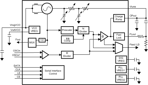
7.3 Feature Description
7.3.1 Reference Oscillator Input
Because the VCO frequency calibration algorithm is based on clocks from the OSCin pin, there are certain bits that need to be set depending on the OSCin frequency. XTLSEL (R6[22:20]) and XTLDIV (R7[9:8]) are both need to be set based on the OSCin frequency, fOSCin. For some options and for low OSCin frequencies, the XTLMAN (R7[21:10]) and XTLMAN2 (R8[4]) words need to be set to the correct value.
Table 1. OSCin Input Impedance (See Figure 1)
| FREQUENCY | POWERED UP (kΩ) | POWERED DOWN (kΩ) | ||||
|---|---|---|---|---|---|---|
| (MHz) | REAL | IMAGINARY | MAGNITUDE | REAL | IMAGINARY | MAGNITUDE |
| 1 | 4.98 | –2.70 | 5.66 | 6.77 | –8.14 | 10.59 |
| 5 | 3.44 | –3.04 | 4.63 | 5.73 | –6.72 | 9.03 |
| 10 | 1.42 | –2.67 | 3.02 | 1.72 | –5.24 | 5.51 |
| 20 | 0.52 | –1.63 | 1.71 | 0.53 | –2.94 | 2.98 |
| 30 | 0.29 | –1.22 | 1.25 | 0.26 | –2.12 | 2.14 |
| 40 | 0.18 | –0.92 | 0.94 | 0.17 | –1.58 | 1.59 |
| 50 | 0.13 | –0.74 | 0.75 | 0.14 | –1.24 | 1.25 |
| 60 | 0.10 | –0.63 | 0.64 | 0.10 | –1.06 | 1.06 |
| 70 | 0.09 | –0.56 | 0.56 | 0.09 | –0.95 | 0.95 |
| 80 | 0.07 | –0.50 | 0.50 | 0.08 | –0.86 | 0.87 |
| 90 | 0.07 | –0.46 | 0.46 | 0.07 | –0.80 | 0.80 |
| 100 | 0.06 | –0.41 | 0.42 | 0.07 | –0.72 | 0.72 |
| 110 | 0.06 | –0.37 | 0.38 | 0.07 | –0.65 | 0.65 |
| 120 | 0.05 | –0.34 | 0.34 | 0.06 | –0.59 | 0.59 |
| 130 | 0.05 | –0.32 | 0.32 | 0.06 | –0.55 | 0.55 |
| 140 | 0.04 | –0.29 | 0.30 | 0.05 | –0.50 | 0.50 |
| 150 | 0.04 | –0.27 | 0.28 | 0.05 | –0.47 | 0.47 |
7.3.2 R Divider
The R divider divides the OSCin frequency down to the phase detector frequency. The R divider value, R, is restricted to the values of 1, 2, 4, 8, 16, and 32. If R is greater than 8, then this also puts restrictions on the fractional denominator, FDEN, than can be used. This is discussed in greater depth in later sections.
7.3.3 Phase Detector and Charge Pump
The phase detector compares the outputs of the R and N dividers and puts out a correction current corresponding to the phase error. The phase detector frequency, fPD, can be calculated as shown in Equation 1.
Choosing R = 1 yields the highest possible phase detector frequency and is optimum for phase noise, although there are restrictions on the maximum phase detector frequency which could force the R value to be larger. The far out PLL noise improves 3 dB for every doubling of the phase detector frequency, but at lower offsets, this effect is much less due to the PLL 1 / f noise. Aside from getting the best PLL phase noise, higher phase detector frequencies also make it easier to filter the noise that the delta-sigma modulator produces, which peaks at an offset frequency of fPD / 2 from the carrier. The LMX2531 also has 16 levels of charge pump currents and a highly flexible fractional modulus. Increasing the charge pump current improves the phase noise about 3 dB per doubling of the charge pump current, although there are small diminishing returns as the charge pump current increases.
From a loop filter design and PLL phase noise perspective, one might think to always design with the highest possible phase detector frequency and charge pump current. However, if one considers the worst case fractional spurs that occur at an output frequency equal to 1 channel spacing away from a multiple of the fOSCin, then this gives reason to reconsider. If the phase detector frequency or charge pump currents are too high, then these spurs could be degraded, and the loop filter may not be able to filter these spurs as well as theoretically predicted. For optimal spur performance, a phase detector frequency around 2.5 MHz and a charge pump current of 1X are recommended.
7.3.4 N Divider and Fractional Circuitry
The N divider in the LMX2531 includes fractional compensation and can achieve any fractional denominator between 1 and 4,194,303. The integer portion, NInteger, is the whole part of the N divider value and the fractional portion, NFractional, is the remaining fraction. So in general, the total N divider value, N, is determined by Equation 2.
For example, if the phase detector frequency (fPD) was 10 MHz and the VCO frequency (fVCO) was 1736.1 MHz, then N would be 173.61. This would imply that NInteger is 173 and NFractional is 61/100. NInteger has some minimum value restrictions that are arise due to the architecture of this divider. The first restrictions arise because the N divider value is actually formed by a quadruple modulus 16/17/20/21 prescaler, which creates minimum divide values. NInteger is further restricted because the LMX2531 due to the fractional engine of the N divider.
The fractional word, NFractional , is a fraction formed with the NUM and DEN words. In the example used here with the fraction of 61/100, NUM = 61 and DEN = 100. The fractional denominator value, DEN, can be set from 2 to 4,194,303. The case of DEN = 0 makes no sense, because this would cause an infinite N value; the case of 1 makes no sense either (but could be done), because integer mode should be used in these applications. All other values in this range, like 10, 32, 42, 734, or 4,000,000 are all valid. Once the fractional denominator, DEN, is determined, the fractional numerator, NUM, is intended to be varied from 0 to DEN-1.
In general, the fractional denominator, DEN, can be calculated by dividing the phase detector frequency by the greatest common divisor (GCD) of the channel spacing (fCH) and the phase detector frequency. If the channel spacing is not obvious, then it can be calculated as the greatest common divisor of all the desired VCO frequencies.
For example, consider the case of a 10 MHz phase detector frequency and a 200 kHz channel spacing at the VCO output. The greatest common divisor of 10 MHz and 200 kHz is just 200 kHz. If one takes 10 MHz divided by 200 kHz, the result is 50. So a fractional denominator of 50, or any multiple of 50 would work in this example. Now consider a case with a 10 MHz phase detector frequency and a 30 kHz channel spacing. The greatest common divisor of 10 MHz and 30 kHz is 10 kHz. The fractional denominator therefore must be a multiple 1000, because this is 10 MHz divided by 10 kHz. For a final example, consider an application with a fixed output frequency of 2110.8 MHz and a OSCin frequency of 19.68 MHz. If the phase detector frequency is chosen to be 19.68 MHz, then the channel spacing can be calculated as the greatest common multiple of 19.68 MHz and 2110.8 MHz, which is 240 kHz. The fractional denominator is therefore a multiple of 41, which is 19.68 MHz / 240 kHz. Refer to AN-1865 Frequency Synthesis and Planning for PLL Architectures (SNAA061) for more details on frequency planning.
To achieve a fractional N value, an integer N divider is modulated between different values. This gives rise to three main degrees of freedom with the LMX2531 delta-sigma engine including the modulator order, dithering, and the way that the fractional portion is expressed. The first degree of freedom is the modulator order, which gives the user the ability to optimize for a particular application. The modulator order can be selected as zero (integer mode), two, three, or four. One simple technique to better understand the impact of the delta-sigma fractional engine on noise and spurs is to tune the VCO to an integer channel and observe the impact of changing the modulator order from integer mode to a higher order. The higher the fractional modulator order is, the lower the spurs theoretically are. However, this is not always the case, and the higher order fractional modulator can sometimes give rise to additional spurious tones, but this is dependent on the application. The second degree of freedom with the LMX2531 delta-sigma engine is dithering. Dithering is often effective in reducing these additional spurious tones, but can add phase noise in some situations. The third degree of freedom is the way that the fraction is expressed. For example, 1/10 can be expressed as 100000/1000000. Expressing the fraction in higher order terms sometimes improves the performance, particularly when dithering is used. In conclusion, there are some guidelines to getting the optimum choice of settings, but these optimum settings are application specific. Refer to AN-1879 Fractional N Frequency Synthesis (SNAA062) for a much more detailed discussion on fractional PLLs and fractional spurs.
7.3.5 Partially Integrated Loop Filter
The LMX2531 integrates the third pole (formed by R3 and C3) and fourth pole (formed by R4 and C4) of the loop filter. The values for C3, C4, R3, and R4 can also be programmed independently through the MICROWIRE interface and also R3 and R4 can be changed during FastLock, for minimum lock time. The larger the values of these components, the stronger the attenuation of the internal loop filter. The maximum attenuation can be achieved by setting R3 = R4 = 40 kΩ and C3 = C4 = 100 pF while the minimum attenuation is achieved by disabling the loop filter by setting EN_LPFLTR (R6[15]) to zero. Note that when the internal loop filter is disabled, there is still a small amount of input capacitance on front of the VCO on the order of 200 pF.
Because that the internal loop filter is on-chip, it is more effective at reducing certain spurs than the external loop filter. The higher order poles formed by the integrated loop filter are also helpful for attenuating noise due to the delta-sigma modulator. This noise produced by the delta-sigma modulator is outside the loop bandwidth and dependent on the modulator order. Although setting the filtering for maximum attenuation gives the best filtering, it puts increased restrictions on how wide the loop bandwidth of the system can be, which corresponds to the case where the shunt loop filter capacitor, C1, is zero. Increasing the charge pump current and/or the phase detector frequency increases the maximum attainable loop bandwidth when designing with the integrated filter. It is recommended to set the internal loop filter as high as possible without restricting the loop bandwidth of the system more than desired. If some setting between the minimum and maximum value is desired, it is preferable to reduce the resistor values before reducing the capacitor values because this will reduce the thermal noise contribution of the loop filter resistors. For design tools and more information on partially integrated loop filters, go to the Clock Design Tool on www.ti.com.
7.3.6 Low Noise, Fully Integrated VCO
The LMX2531 includes a fully integrated VCO, including the inductors. For optimum phase noise performance, this VCO has frequency and phase noise calibration algorithms. The frequency calibration algorithm is necessary because the VCO internally divides up the frequency range into several bands, to achieve a lower tuning gain, and therefore better phase noise performance. The frequency calibration routine is activated any time that the R0 register is programmed. There are several bits including LOCKMODE and XTLSEL that need to be set properly for this calibration to be performed in a reliable fashion. If the temperature shifts considerably and the R0 register is not programmed, then it cannot drift more than the maximum allowable drift for continuous lock, ΔTCL, or else the VCO is not ensured to stay in lock. The phase noise calibration algorithm is necessary to achieve the lowest possible phase noise. Each version of the LMX2531, the VCO_ACI_SEL bit (R6[19:16]) needs to be set to the correct value to ensure the best possible phase noise.
The gain of the VCO can change considerably over frequency. It is lowest at the minimum frequency and highest at the maximum frequency. This range is specified in Electrical Characteristics of the data sheet. When designing the loop filter, the following method is recommended to determine what VCO gain to design to. First, take the geometric mean of the minimum and maximum frequencies that are to be used. Then use a linear approximation to extrapolate the VCO gain. Suppose the application requires the LMX2531LQ2080E PLL to tune from 2100 to 2150 MHz. The geometric mean of these frequencies is sqrt (2100 × 2150) MHz = 2125 MHz. The VCO gain is specified as 9 MHz/V at 1904 MHz and 20 MHz/V at 2274 MHz. Over this range of 370 MHz, the VCO gain changes 11 MHz/V. Therefore, at 2125 MHz, the VCO gain would be approximately 9 + (2125 – 1904) × 11 / 370 = 15.6 MHz/V. Although the VCO gain can change from part to part, this variation is small compared to how much the VCO gain can change over frequency.
The VCO frequency is related to the other frequencies and divider values as shown in Equation 4.
7.3.7 Programmable VCO Divider
All options of the LMX2531 offer the option of dividing the VCO output by two to get half of the VCO frequency at the Fout pin. The channel spacing at the Fout pin is also divided by two as well. Because this divide by two is outside feedback path between the VCO and the PLL, enabling does require one to change the N divider, R divider, or loop filter values. When this divider is enabled, there will be some far-out phase noise contribution to the VCO noise. Note that the R0 register should be reprogrammed the first time after the DIV2 bit is enabled or disabled for optimal phase noise performance. The frequency at the Fout pin is related to the VCO frequency and divider value, D, as shown in Equation 5.
7.3.8 Serial Data Timing Requirements
See MICROWIRE Timing Requirements.
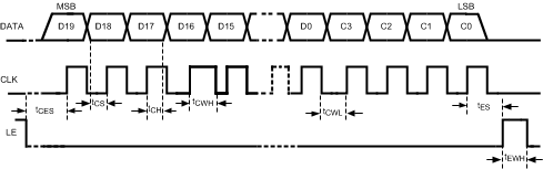 Figure 2. Serial Data Timing Diagram
The DATA is clocked into a shift register on each rising edge of the CLK signal. On the rising edge of the LE signal, the data is sent from the shift registers to an actual counter. There are several other considerations as well:
- A slew rate of at least 30 V/μs is recommended for the CLK, DATA, and LE signals.
- After the programming is complete, the CLK, DATA, and LE signals should be returned to a low state.
- It is recommended to put a small delay between the falling edge of the last CLK pulse and the rising edge of the LE pulse for optimal noise immunity and the most reliable programming.
- Although it is strongly recommended to keep LE low after programming, LE can be kept high if bit R5[23] is changed to 0 (from its default value of 1). If this bit is changed, then the operation of the part is not ensured because it is not tested under these conditions.
- If the CLK and DATA lines are toggled while the in VCO is in lock, as is sometimes the case when these lines are shared with other parts, the phase noise may be degraded during the time of this programming.
- If the part is not programmed, the values of the registers in this part have to be assumed to be random. Therefore, the current consumption and spurs generated by this part can be random. If this is an issue, the CE pin can be held low for more consistent behavior.
7.4 Device Functional Modes
The LMX2531 operates mainly in the active mode. The other two modes are reset and powerdown modes. The powerdown mode can be achieved by taking the CE pin to 0 V. The reset mode is achieved if the REG_RST bit is set to 1.
7.5 Programming
The LMX2531 is programmed using 11 24-bit registers used to control the LMX2531 operation. A 24-bit shift register is used as a temporary register to indirectly program the on-chip registers. The shift register consists of a data field and an address field. The last 4 register bits, CTRL[3:0] form the address field, which is used to decode the internal register address. The remaining 20 bits form the data field DATA[19:0]. While LE is low, serial data is clocked into the shift register upon the rising edge of clock (data is programmed MSB first). When LE goes high, data is transferred from the data field into the selected register bank. Although there are actually 14 registers in this part, only a portion of them should be programmed, because the state of the other hidden registers (R13, R11, and R10) are set during the initialization sequence. Although it is possible to program these hidden registers, as well as a lot of bits that are defined to either 1 or 0, the user should not experiment with these hidden registers and bits, because the parts are not tested under these conditions and doing so will most likely degrade performance.
Table 2. Register Location Truth Table
| C3 | C2 | C1 | C0 | Data Address |
|---|---|---|---|---|
| 1 | 1 | 0 | 0 | R12 |
| 1 | 0 | 0 | 1 | R9 |
| 1 | 0 | 0 | 0 | R8 |
| 0 | 1 | 1 | 1 | R7 |
| 0 | 1 | 1 | 0 | R6 |
| 0 | 1 | 0 | 1 | R5 |
| 0 | 1 | 0 | 0 | R4 |
| 0 | 0 | 1 | 1 | R3 |
| 0 | 0 | 1 | 0 | R2 |
| 0 | 0 | 0 | 1 | R1 |
| 0 | 0 | 0 | 0 | R0 |
7.6 Register Maps
7.6.1 General Programming Information
Table 3. Programming Register Structure
| DATA[19:0] | CONTROL[3:0] | ||||||||||||||||||||||
|---|---|---|---|---|---|---|---|---|---|---|---|---|---|---|---|---|---|---|---|---|---|---|---|
| MSB | LSB | ||||||||||||||||||||||
| D19 | D18 | D17 | D16 | D15 | D14 | D13 | D12 | D11 | D10 | D9 | D8 | D7 | D6 | D5 | D4 | D3 | D2 | D1 | D0 | C3 | C2 | C1 | C0 |
7.6.1.1 Initialization Sequence
The initial loading sequence from a cold start is described in Table 4. The registers must be programmed in order shown. There must be a minimum of 10 ms between the time when R5 is last loaded and R1 is loaded to ensure time for the LDOs to power up properly.
Table 4. Initialization Sequence
| REG. | 23 | 22 | 21 | 20 | 19 | 18 | 17 | 16 | 15 | 14 | 13 | 12 | 11 | 10 | 9 | 8 | 7 | 6 | 5 | 4 | 3 | 2 | 1 | 0 |
|---|---|---|---|---|---|---|---|---|---|---|---|---|---|---|---|---|---|---|---|---|---|---|---|---|
| DATA[19:0] | C3 | C2 | C1 | C0 | ||||||||||||||||||||
| R5 INIT1 |
1 | 0 | 0 | 0 | 0 | 1 | 0 | 0 | 0 | 0 | 0 | 0 | 0 | 0 | 0 | 0 | 0 | 0 | 0 | 0 | 0 | 1 | 0 | 1 |
| R5 INIT2 |
1 | 0 | 0 | 0 | 0 | 0 | 0 | 0 | 0 | 0 | 0 | 0 | 0 | 0 | 0 | 0 | 0 | 0 | 0 | 0 | 0 | 1 | 0 | 1 |
| R5 | 1 | 0 | 0 | 0 | 0 | 0 | 0 | 0 | 0 | 0 | 0 | 0 | 0 | 1 | 1 | 1 | 1 | 1 | 1 | 1 | 0 | 1 | 0 | 1 |
| R12 | Program R12 as shown in the complete register map. | 1 | 1 | 0 | 0 | |||||||||||||||||||
| R9 | Program R9 as shown in the complete register map. | 1 | 0 | 0 | 1 | |||||||||||||||||||
| R8 | See individual section for Register R8 programming information. Programming of this register is necessary under specific circumstances. |
1 | 0 | 0 | 0 | |||||||||||||||||||
| R7 | See individual section for Register R7 programming information. | 0 | 1 | 1 | 1 | |||||||||||||||||||
| R6 | See individual section for Register R6 programming information. | 0 | 1 | 1 | 0 | |||||||||||||||||||
| R4 | See individual section for Register R4 programming information. Register R4 only needs to be programmed if FastLock is used. |
0 | 1 | 0 | 0 | |||||||||||||||||||
| R3 | See individual section for Register R3 programming information. | 0 | 0 | 1 | 1 | |||||||||||||||||||
| R2 | See individual section for Register R2 programming information. | 0 | 0 | 1 | 0 | |||||||||||||||||||
| R1 | See individual section for Register R1 programming information. | 0 | 0 | 0 | 1 | |||||||||||||||||||
| R0 | See individual section for Register R0 programming information. | 0 | 0 | 0 | 0 | |||||||||||||||||||
7.6.1.2 Complete Register Content Map
Table 5 shows all the programmable bits for the LMX2531. No programming order or initialization sequence is implied by Table 5, only the location of the programming information.
Table 5. Complete Register Content Map
| REGISTER | 23 | 22 | 21 | 20 | 19 | 18 | 17 | 16 | 15 | 14 | 13 | 12 | 11 | 10 | 9 | 8 | 7 | 6 | 5 | 4 | 3 | 2 | 1 | 0 |
| DATA[19:0] | C3 | C2 | C1 | C0 | ||||||||||||||||||||
| R0 | N [7:0] |
NUM [11:0] |
0 | 0 | 0 | 0 | ||||||||||||||||||
| R1 | 0 | 0 | 1 | ICP [3:0] |
N [10:8] |
NUM [21:12] |
0 | 0 | 0 | 1 | ||||||||||||||
| R2 | 0 | 1 | DEN [11:0] |
R [5:0] |
0 | 0 | 1 | 0 | ||||||||||||||||
| R3 | DIV2 | FDM | DITHER [1:0] |
ORDER [1:0] |
FoLD [3:0] |
DEN [21:12] |
0 | 0 | 1 | 1 | ||||||||||||||
| R4 | 0 | 0 | ICPFL [3:0] |
TOC [13:0] |
0 | 1 | 0 | 0 | ||||||||||||||||
| R5 | 1 | 0 | 0 | 0 | 0 | REG_RST | 0 | 0 | 0 | 0 | 0 | 0 | 0 | EN_DIGLDO | EN_PLLLDO2 | EN_PLLLDO1 | EN_VCOLD | EN_OSC | EN_VCO | EN_PLL | 0 | 1 | 0 | 1 |
| R6 | 0 | XTLSEL [2:0] |
VCO_ACI_SEL [3:0] |
EN_LPFLTR | R4_ADJ [1:0] |
R4_ADJ_FL [1:0] |
R3_ADJ [1:0] |
R3_ADJ_FL [1:0] |
C3_4_ADJ [2:0] |
0 | 1 | 1 | 0 | |||||||||||
| R7 | 0 | 0 | XTLMAN [11:0] |
XTLDIV [1:0] |
0 | 0 | 0 | 0 | 0 | 1 | 1 | 1 | ||||||||||||
| R8 | 0 | 0 | 0 | 0 | 0 | 0 | 1 | LOCK MODE |
0 | 0 | 0 | 0 | 0 | 0 | 0 | 0 | 0 | 0 | XTL MAN2 |
1 | 0 | 0 | 0 | |
| R9 | 0 | 0 | 0 | 0 | 0 | 0 | 0 | 0 | 0 | 0 | 0 | 0 | 1 | 0 | 1 | 1 | 1 | 0 | 1 | 0 | 1 | 0 | 0 | 1 |
| R12 | 0 | 0 | 0 | 0 | 0 | 0 | 0 | 1 | 0 | 0 | 0 | 0 | 0 | 1 | 0 | 0 | 1 | 0 | 0 | 0 | 1 | 1 | 0 | 0 |
7.6.1.3 Register R0
The action of programming the R0 register activates a frequency calibration routine for the VCO. This calibration is necessary to get the VCO to center the tuning voltage for optimal performance. If the temperature drifts considerably, then the PLL should stay in lock, provided that the temperature drift specification is not violated.
7.6.1.3.1 NUM[10:0] and NUM[21:12] -- Fractional Numerator
The NUM word is split between the R0 register and R1 register. The Numerator bits determine the fractional numerator for the delta-sigma PLL. This value can go from 0 to 4095 when the FDM bit (R3[22]) is 0 (the other bits in this register are ignored), or 0 to 4194303 when the FDM bit is 1.
Table 6. Fractional Numerator
| FRACTIONAL NUMERATOR |
NUM[21:12] | NUM[11:0] | ||||||||||||||||||||
|---|---|---|---|---|---|---|---|---|---|---|---|---|---|---|---|---|---|---|---|---|---|---|
| 0 | 0 | 0 | 0 | 0 | 0 | 0 | 0 | 0 | 0 | 0 | 0 | 0 | 0 | 0 | 0 | 0 | 0 | 0 | 0 | 0 | 0 | 0 |
| ... | ||||||||||||||||||||||
| 409503 | 1 | 1 | 1 | 1 | 1 | 1 | 1 | 1 | 1 | 1 | 1 | 1 | 1 | 1 | 1 | 1 | 1 | 1 | 1 | 1 | 1 | 1 |
| 4096 | 0 | 0 | 0 | 0 | 0 | 0 | 0 | 0 | 0 | 0 | 1 | 0 | 0 | 0 | 0 | 0 | 0 | 0 | 0 | 0 | 0 | 0 |
| ... | ||||||||||||||||||||||
| 4194303 | 1 | 1 | 1 | 1 | 1 | 1 | 1 | 1 | 1 | 1 | 1 | 1 | 1 | 1 | 1 | 1 | 1 | 1 | 1 | 1 | 1 | 1 |
Note that there are restrictions on the fractional numerator value depending on the R divider value if it is 16 or 32.
7.6.1.3.2 N[7:0] and N[10:8]
The N counter is 11 bits. 8 of these bits are located in the R0 register, and the remaining 3 (MSB bits) are located in the R1 register. The LMX2531 consists of an A, B, and C counter, which work in conjunction with the 16/17/20/21 prescaler to form the final N counter value.
Table 7. N Divider Value
| N[10:8] | N[7:0] | ||||||||||
|---|---|---|---|---|---|---|---|---|---|---|---|
| N Value | C | B | A | ||||||||
| <48 | Values less than 48 are prohibited. | ||||||||||
| 48 - 51 | Possible ONLY with ORDER = 1 (Reset Modulator) | ||||||||||
| 52-54 | Values of 52 - 54 are prohibited. | ||||||||||
| 55 | 0 | 0 | 0 | 0 | 0 | 1 | 1 | 0 | 1 | 1 | 1 |
| ... | |||||||||||
| 2039 | 1 | 1 | 1 | 1 | 1 | 1 | 1 | 0 | 1 | 1 | 1 |
7.6.1.4 Register R1
7.6.1.4.1 NUM[21:12]
These are the MSB bits in for the fractional numerator that already have been described.
7.6.1.4.2 N[10:8] -- 3 MSB Bits for the N Counter
These are the 2 MSB bits for the N counter, which were discussed in Register R0.
7.6.1.4.3 ICP[3:0] -- Charge Pump Current
This bit programs the charge pump current in from 90 µA to 1440 µA in 90 µA steps. In general, higher charge pump currents yield better phase noise for the PLL, but also can cause higher spurs.
Table 8. Charge Pump Current
| ICP | CHARGE PUMP STATE | TYPICAL CHARGE PUMP CURRENT at 3 VOLTS (µA) |
|---|---|---|
| 0 | 1X | 90 |
| 1 | 2X | 180 |
| 2 | 3X | 270 |
| 3 | 4X | 360 |
| 4 | 5X | 450 |
| 5 | 6X | 540 |
| 6 | 7X | 630 |
| 7 | 8X | 720 |
| 8 | 9X | 810 |
| 9 | 10X | 900 |
| 10 | 11X | 990 |
| 11 | 12X | 1080 |
| 12 | 13X | 1170 |
| 13 | 14X | 1260 |
| 14 | 15X | 1350 |
| 15 | 16X | 1440 |
7.6.1.5 Register R2
7.6.1.5.1 R[5:0] -- R Counter Value
These bits determine the phase detector frequency. The OSCin frequency is divided by this R counter value. Note that only the values of 1, 2, 4, 8, 16, and 32 are allowed.
Table 9. R Divider Value
| R VALUE | FRACTIONAL DENOMINATOR RESTRICTIONS |
R[5:0] | |||||
|---|---|---|---|---|---|---|---|
| 0,3,5-7, 9-15,17-31, 33-63 |
n/a | These values are illegal. | |||||
| 1 | none | 0 | 0 | 0 | 0 | 0 | 1 |
| 2 | none | 0 | 0 | 0 | 0 | 1 | 0 |
| 4 | none | 0 | 0 | 0 | 1 | 0 | 0 |
| 8 | none | 0 | 0 | 1 | 0 | 0 | 0 |
| 16 | Must be divisible by 2 | 0 | 1 | 0 | 0 | 0 | 0 |
| 32 | Must be divisible by 4 | 1 | 0 | 0 | 0 | 0 | 0 |
The R counter value can put some restrictions on the fractional denominator. In the case that it is 16, the fractional denominator must be divisible by 2, which is equivalent to saying that the LSB of the fractional denominator word is zero. In the case that the R counter is 32, the two LSB bits of the fractional denominator word must also be zero, which is equivalent to saying that the fractional denominator must be divisible by 4. Because the fractional denominator can be very large, this should cause no issues. For instance, if one wanted to achieve a fractional word of 1/65, and the R counter value was 16, the fractional word could be changed to 4/260, and the same resolution could be achieved.
7.6.1.5.2 DEN[21:12] and DEN[11:0]-- Fractional Denominator
These bits determine the fractional denominator. Note that the MSB bits for this word are in register R3. If the FDM bit is set to 0, DEN[21:12] are ignored. The fractional denominator should only be set to zero if the fractional circuitry is being disabled by setting ORDER = 1. A value of one never makes sense to use. All other values could reasonably be used in fractional mode.
Table 10. Fractional Denominator
| FRACTIONAL DENOMINATOR |
DEN[21:12] | DEN[11:0] | ||||||||||||||||||||
|---|---|---|---|---|---|---|---|---|---|---|---|---|---|---|---|---|---|---|---|---|---|---|
| 0 | 0 | 0 | 0 | 0 | 0 | 0 | 0 | 0 | 0 | 0 | 0 | 0 | 0 | 0 | 0 | 0 | 0 | 0 | 0 | 0 | 0 | 0 |
| ... | ||||||||||||||||||||||
| 4095 | 1 | 1 | 1 | 1 | 1 | 1 | 1 | 1 | 1 | 1 | 1 | 1 | 1 | 1 | 1 | 1 | 1 | 1 | 1 | 1 | 1 | 1 |
| 4096 | 0 | 0 | 0 | 0 | 0 | 0 | 0 | 0 | 0 | 1 | 0 | 0 | 0 | 0 | 0 | 0 | 0 | 0 | 0 | 0 | 0 | 0 |
| ... | ||||||||||||||||||||||
| 4194303 | 1 | 1 | 1 | 1 | 1 | 1 | 1 | 1 | 1 | 1 | 1 | 1 | 1 | 1 | 1 | 1 | 1 | 1 | 1 | 1 | 1 | 1 |
7.6.1.6 Register R3
7.6.1.6.1 DEN[21:12] -- Extension for the Fractional Denominator
These are the MSB bits of the DEN word, which have already been discussed.
7.6.1.6.2 FoLD[3:0] -- Multiplexed Output for Ftest/LD Pin
The FoLD[3:0] word is used to program the output of the Ftest/LD pin. This pin can be used for a general purpose I/O pin, a lock detect pin, and for diagnostic purposes. When programmed to the digital lock detect state, the output of the Ftest/LD pin will be high when the part is in lock, and low otherwise. Lock is determined by comparing the input phases to the phase detector. The analog lock detect modes put out a high signal with very fast negative pulses, that correspond to when the charge pump comes on. This output can be low pass filtered with an RC filter to determine the lock detect state. If the open drain state is used, a additional pullup resistor is required. For diagnostic purposes, the options that allow one to view the output of the R counter or the N counter can be very useful. Be aware that the output voltage level of the Ftest/LD is not equal to the supply voltage of the part, but rather is given by VOH and VOL in Electrical Characteristics.
Table 11. Ftest/LD Pin Functions
| FoLD | OUTPUT TYPE | FUNCTION |
|---|---|---|
| 0 | High Impedance | Disabled |
| 1 | Push-Pull | Logical High State |
| 2 | Push-Pull | Logical Low State |
| 3 | Push-Pull | Digital Lock Detect |
| 4 | N/A | Reserved |
| 5 | Push-Pull | N Counter Output Divided by 2 |
| 6 | Open-Drain | Analog Lock Detect |
| 7 | Push-Pull | Analog Lock Detect |
| 8 | N/A | Reserved |
| 9 | N/A | Reserved |
| 10 | N/A | Reserved |
| 11 | N/A | Reserved |
| 12 | N/A | Reserved |
| 13 | N/A | Reserved |
| 14 | Push-Pull | R Counter Output |
| 15 | N/A | Reserved |
7.6.1.6.3 ORDER -- Order of Delta-Sigma Modulator
This bit determines the order of the delta-sigma modulator in the PLL. In general, higher order fractional modulators tend to reduce the primary fractional spurs that occur at increments of the channel spacing, but can also create spurs that are at a fraction of the channel spacing, if there is not sufficient filtering. The optimal choice of modulator order is very application specific, however, a third order modulator is a good starting point if not sure what to try first.
Table 12. Delta-Sigma Modulator
| ORDER | DELTA-SIGMA MODULATOR ORDER |
|---|---|
| 0 | Fourth |
| 1 | Reset Modulator (Integer Mode - all fractions are ignored) |
| 2 | Second |
| 3 | Third |
7.6.1.6.4 DITHER -- Dithering
Dithering is useful in reducing fractional spurs, especially those that occur at a fraction of the channel spacing. The only exception is when the fractional numerator is zero. In this case, dithering usually is not a benefit. Dithering also can sometimes increase the PLL phase noise by a fraction of a dB. In general, if dithering is disabled, phase noise may be slightly better inside the loop bandwidth of the system, but spurs are likely to be worse too.
Table 13. Fractional Dithering
| DITHER | DITHERING MODE |
|---|---|
| 0 | Weak Dithering |
| 1 | Reserved |
| 2 | Strong Dithering |
| 3 | Dithering Disabled |
7.6.1.6.5 FDM -- Fractional Denominator Mode
When this bit is set to 1, the 10 MSB bits for the fractional numerator and denominator are considered. This allows the fractional denominator to range from 1 to 4,194,303. If this bit is set to zero, only the 12 LSB bits of the fractional numerator and denominator are considered, and this allows a fractional denominator from 1 to 4095. When this bit is disabled, the current consumption is about 0.5 mA lower.
7.6.1.6.6 DIV2
When this bit is enabled, the output of the VCO is divided by 2. Enabling this bit does have some impact on harmonic content and output power.
Table 14. VCO Output Divider
| DIV2 | VCO OUTPUT FREQUENCY |
|---|---|
| 0 | Not Divided by 2 |
| 1 | Divided by 2 |
7.6.1.7 Register R4
7.6.1.7.1 TOC[13:0] -- Time-Out Counter for FastLock
When the value of this word is 3 or less, then FastLock is disabled, and this pin can only be used for general purpose I/O. When this value is 4 or greater, the time-out counter is engaged for the amount of phase detector cycles shown in Table 15.
Table 15. FastLock Timeout Counter
| TOC VALUE | FLout PIN STATE | TIMEOUT COUNT |
|---|---|---|
| 0 | High Impedance | 0 |
| 1 | Low | Always Enabled |
| 2 | Low | 0 |
| 3 | High | 0 |
| 4 | Low | 4 × 2 Phase Detector |
| . | . | . |
| 16383 | Low | 16383 × 2 Phase Detector |
When this count is active, the FLout pin is grounded, the FastLock current is engaged, and the resistors R3 and R4 are also potentially changed. The table below summarizes the bits that control various values in and out of FastLock differences.
Table 16. FastLock Filter Values
| FastLock STATE | FLout | CHARGE PUMP CURRENT | R3 | R4 |
|---|---|---|---|---|
| Steady State | High Impedance | ICP | R3_ADJ | R4_ADJ |
| Fastlock | Grounded | ICPFL | R3_ADJ_FL | R4_ADJ_FL |
7.6.1.7.2 ICPFL[3:0] -- Charge Pump Current for Fastlock
When FastLock is enabled, this is the charge pump current that is used for faster lock time.
Table 17. FastLock Charge Pump Current
| ICPFL | Fastlock CHARGE PUMP STATE | TYPICAL Fastlock CHARGE PUMP CURRENT at 3 VOLTS (µA) |
|---|---|---|
| 0 | 1X | 90 |
| 1 | 2X | 180 |
| 2 | 3X | 270 |
| 3 | 4X | 360 |
| 4 | 5X | 450 |
| 5 | 6X | 540 |
| 6 | 7X | 630 |
| 7 | 8X | 720 |
| 8 | 9X | 810 |
| 9 | 10X | 900 |
| 10 | 11X | 990 |
| 11 | 12X | 1080 |
| 12 | 13X | 1170 |
| 13 | 14X | 1260 |
| 14 | 15X | 1350 |
| 15 | 16X | 1440 |
7.6.1.8 Register R5
7.6.1.8.1 EN_PLL -- Enable Bit for PLL
When this bit is set to 1 (default), the PLL is powered up, otherwise, it is powered down.
7.6.1.8.2 EN_VCO -- Enable Bit for the VCO
When this bit is set to 1 (default), the VCO is powered up, otherwise, it is powered down.
7.6.1.8.3 EN_OSC -- Enable Bit for the Oscillator Inverter
When this bit is set to 1 (default), the reference oscillator is powered up, otherwise it is powered down.
7.6.1.8.4 EN_VCOLDO -- Enable Bit for the VCO LDO
When this bit is set to 1 (default), the VCO LDO is powered up, otherwise it is powered down.
7.6.1.8.5 EN_PLLLDO1 -- Enable Bit for the PLL LDO 1
When this bit is set to 1 (default), the PLL LDO 1 is powered up, otherwise it is powered down.
7.6.1.8.6 EN_PLLLDO2 -- Enable Bit for the PLL LDO 2
When this bit is set to 1 (default), the PLL LDO 2 is powered up, otherwise it is powered down.
7.6.1.8.7 EN_DIGLDO -- Enable Bit for the digital LDO
When this bit is set to 1 (default), the Digital LDO is powered up, otherwise it is powered down.
7.6.1.8.8 REG_RST -- Resets All Registers to Default Settings
This bit needs to be programmed three times to initialize the part. When this bit is set to one, all registers are set to default mode, and the part is powered down. The second time the R5 register is programmed with REG_RST = 0, the register reset is released and the default states are still in the registers. However, because the default states for the blocks and LDOs is powered off, it is therefore necessary to program R5 a third time so that all the LDOs and blocks can be programmed to a power up state. When this bit is set to 1, all registers are set to the default modes, but part is powered down. For normal operation, this bit is set to 0. Once this initialization is done, it is not necessary to do this again unless power is removed from the device.
7.6.1.9 Register R6
7.6.1.9.1 C3_C4_ADJ[2:0] -- Value FOR C3 and C4 In The Internal Loop Filter
Table 18. Internal Loop Filter Capacitors
| C3_C4_ADJ | C3 (pF) | C4 (pF) |
|---|---|---|
| 0 | 50 | 50 |
| 1 | 50 | 100 |
| 2 | 50 | 150 |
| 3 | 100 | 50 |
| 4 | 150 | 50 |
| 5 | 100 | 100 |
| 6 | 50 | 150 |
| 7 | 50 | 150 |
7.6.1.9.2 R3_ADJ_FL[1:0] -- Value for Internal Loop Filter Resistor R3 During Fastlock
Table 19. Internal Loop Filter Resistor R3 During Fastlock
| R3_ADJ_FL Value | R3 RESISTOR DURING Fastlock (kΩ) |
|---|---|
| 0 | 10 |
| 1 | 20 |
| 2 | 30 |
| 3 | 40 |
7.6.1.9.3 R3_ADJ[1:0] -- Value for Internal Loop Filter Resistor R3
Table 20. Internal Loop Filter Resistor R3
| R3_ADJ | R3 VALUE (kΩ) |
|---|---|
| 0 | 10 |
| 1 | 20 |
| 2 | 30 |
| 3 | 40 |
7.6.1.9.4 R4_ADJ_FL[1:0] -- Value for Internal Loop Filter Resistor R4 During Fastlock
Table 21. Internal Loop Filter Resistor R4 During FastLock
| R4_ADJ_FL | R4 VALUE DURING Fast Lock (kΩ) |
|---|---|
| 0 | 10 |
| 1 | 20 |
| 2 | 30 |
| 3 | 40 |
7.6.1.9.5 R4_ADJ[1:0] -- Value for Internal Loop Filter Resistor R4
Table 22. Internal Loop Filter Resistor R4
| R4_ADJ | R4 VALUE (kΩ) |
|---|---|
| 0 | 10 |
| 1 | 20 |
| 2 | 30 |
| 3 | 40 |
7.6.1.9.6 EN_LPFLTR-- Enable for Partially Integrated Internal Loop Filter
The Enable Loop Filter bit is used to enable or disable the third and fourth pole on-chip loop filters.
Table 23. Enable Bit for Internal Loop Filter
| EN_LPFLTR | 3rd and 4th POLES of LOOP FILTER |
|---|---|
| 0 | disabled (R3 = R4 = 0 Ω and C3 + C4 = 200 pF) |
| 1 | enabled |
7.6.1.9.7 VCO_ACI_SEL
This bit is used to optimize the VCO phase noise. The recommended values are what are used for all testing purposes, and this bit should be set as instructed in the following table.
Table 24. VCO ACI Selection
| PART | VCO_ACI_SEL |
|---|---|
| All Other Options | 8 |
| LMX2531LQ2265E LMX2531LQ2570E LMX2531LQ2820E LMX2531LQ3010E |
6 |
7.6.1.9.8 XTLSEL[2:0] -- OSCin Select
The XTLSEL bit is used to select between manual oscin mode and one of the automatic modes. The user may choose manual oscin mode (XTLSEL = 4) and program the XTLMAN (R7[21:10]) and XTLMAN2 (R7[4]) bits for a specific OSCin frequency, or one of the automatic modes (XTLSEL = 0, 1, 2, 3). For the LMX2531LQ2080E/2570E options or when the OSCin frequency is less than 8 MHz, manual oscin mode must always be selected. The automatic modes can be used for the other frequency options. When using one of the automatic modes, XTLSEL should be set based on the OSCin frequency.
Table 25. OSCin Frequency Select
| XTLSEL | MODE | OSCin FREQUENCY |
|---|---|---|
| 0 | Automatic Modes
Programming of XTLMAN (R7[21:10]) not required. Programming of XTLMAN2 (R7[4]) not required. |
8 — 25 MHz |
| 1 | 25 — 50 MHz | |
| 2 | 50 — 70 MHz | |
| 3 | 70 — 80 MHz | |
| 4 | Manual OSCin Mode
Must use this for LMX2531LQ2080E/2570E/2820E/3010E Must use this if fOSCin < 8 MHz Programming of XTLMAN (R7[21:10]) required. Programming of XTLMAN2 (R7[4]) may be required. |
5 — 80 MHz |
| 5, 6, 7 | Reserved | |
7.6.1.10 Register R7
7.6.1.10.1 XTLDIV[1:0] -- Division Ratio for the OSCin Frequency
The frequency provided to the VCO frequency calibration circuitry is based on the OSCin frequency divided down by a factor, determined by the XTLDIV word. Note that this division ratio is independent of the R counter value or the phase detector frequency. The necessary division ratio depends on the OSCin frequency and is shown in Table 26.
Table 26. OSCin Division Ratio
| XTLDIV | OSCin DIVISION RATIO | OSCin RANGE |
|---|---|---|
| 0 | Reserved | Reserved |
| 1 | Divide by 2 | < 20 MHz |
| 2 | Divide by 4 | 20 — 40 MHz |
| 3 | Divide by 8 | > 40 MHz |
7.6.1.10.2 XTLMAN[11:0] -- Manual OSCin Mode
XTLMAN must be programmed if word XTLSEL (XTLSEL[2:0] -- OSCin Select) is set to manual OSCin mode. In the table below, the proper value for XTLMAN is shown based on some common OSCin frequencies (fOSCin) and various LMX2531 options. For any OSCin frequency XTLMAN can be calculated as 16 × fOSCin / Kbit. fOSCin is expressed in MHz and Kbit values for the LMX2531 frequency options can be found in Table 28.
Table 27. XTLMAN Values for Common OSCin Frequencies
| DEVICE | fOSCin | |||||
|---|---|---|---|---|---|---|
| 5 MHz | 10 MHz | 20 MHz | 30.72 MHz | 61.44 MHz | 76.8 MHz | |
| LMX2531LQ1146E | 53 | 107 | 213 | 327 | 655 | 819 |
| LMX2531LQ1226E | 53 | 107 | 213 | 327 | 655 | 819 |
| LMX2531LQ1312E | 47 | 94 | 188 | 289 | 578 | 722 |
| LMX2531LQ1415E | 47 | 94 | 188 | 289 | 578 | 722 |
| LMX2531LQ1500E | 40 | 80 | 160 | 246 | 492 | 614 |
| LMX1531LQ1515E | 40 | 80 | 160 | 246 | 492 | 614 |
| LMX2531LQ1570E | 38 | 76 | 152 | 234 | 468 | 585 |
| LMX2531LQ1650E | 38 | 76 | 152 | 234 | 468 | 585 |
| LMX2531LQ1700E | 35 | 70 | 139 | 214 | 427 | 534 |
| LMX2531LQ1742 | 32 | 64 | 128 | 197 | 393 | 492 |
| LMX2531LQ1778E | 31 | 62 | 123 | 189 | 378 | 473 |
| LMX2531LQ1910E | 27 | 53 | 107 | 164 | 328 | 410 |
| LMX2531LQ2265E | 20 | 40 | 80 | 123 | 246 | 307 |
| LMX2531LQ2080E | 18 | 36 | 71 | 109 | 218 | 273 |
| LMX2531LQ2570E | 13 | 27 | 53 | 82 | 164 | 205 |
| LMX2531LQ2820E | 11 | 23 | 46 | 70 | 140 | 178 |
| LMX2531LQ3010E | 10 | 20 | 40 | 61 | 123 | 154 |
Table 28. Kbit Values for Various LMX2531 Options
| DEVICE | Kbit |
|---|---|
| LMX2531LQ1146E | 1.5 |
| LMX2531LQ1226E | 1.5 |
| LMX2531LQ1312E | 1.7 |
| LMX2531LQ1415E | 1.7 |
| LMX2531LQ1500E | 2 |
| LMX2531LQ1515E | 2 |
| LMX2531LQ1570E | 2.1 |
| LMX2531LQ1650E | 2.1 |
| LMX2531LQ1700E | 2.3 |
| LMX25311742 | 2.5 |
| LMX2531LQ1778E | 2.6 |
| LMX2531LQ1910E | 3 |
| LMX2531LQ2265E | 4 |
| LMX2531LQ2080E | 4.5 |
| LMX2531LQ2570E | 6 |
| LMX2531LQ2820E | 7 |
| LMX2531LQ3010E | 8 |
7.6.1.11 Register R8
7.6.1.11.1 XTLMAN2 -- Manual Crystal Mode Second Adjustment
This bit also adjusts the calibration timing for lock time. In the case that manual mode for XTLSEL is selected and the OSCin frequency is greater than 40 MHz, this bit should be enabled, otherwise it should be 0.
7.6.1.11.2 LOCKMODE -- Frequency Calibration Mode
This bit controls the method for which the VCO frequency calibration is done. The two valid modes are linear mode and mixed mode. Linear mode works by searching through the VCO frequency bands in a consecutive manner. Mixed mode works by initially using a divide and conquer approach and then using a linear approach. For small frequency changes, linear mode is faster and for large frequency changes, mixed mode is faster. Linear mode can always be used, but there are restrictions for when Mixed Mode can be used.
Table 29. Lockmode Settings
| LOCKMODE | DESCRIPTION | CONDITIONS on OPTIONS | CONDITIONS on OSCin FREQUENCY |
|---|---|---|---|
| 0 | Reserved | Never use this mode | |
| 1 | Linear Mode | Works over all options and all valid OSCin Frequencies | |
| 2 | Mixed Mode | All but the following options LMX2531LQ1146E/1226E/1312E/1415E/1515E |
fOSCin ≥ 8 MHz |
| 3 | Reserved | Never use this mode | |
7.6.1.12 Register R9
All the bits in this register should be programmed as shown in Complete Register Content Map.
7.6.1.13 Register R12
Even though this register does not have user-selectable bits, it still needs to be programmed. This register should be loaded as shown in Complete Register Content Map.