SNAS252S October 2005 – December 2014 LMX2531
PRODUCTION DATA.
- 1 Features
- 2 Applications
- 3 Description
- 4 Revision History
- 5 Pin Configuration and Functions
- 6 Specifications
-
7 Detailed Description
- 7.1 Overview
- 7.2 Functional Block Diagram
- 7.3 Feature Description
- 7.4 Device Functional Modes
- 7.5 Programming
- 7.6
Register Maps
- 7.6.1
General Programming Information
- 7.6.1.1 Initialization Sequence
- 7.6.1.2 Complete Register Content Map
- 7.6.1.3 Register R0
- 7.6.1.4 Register R1
- 7.6.1.5 Register R2
- 7.6.1.6 Register R3
- 7.6.1.7 Register R4
- 7.6.1.8
Register R5
- 7.6.1.8.1 EN_PLL -- Enable Bit for PLL
- 7.6.1.8.2 EN_VCO -- Enable Bit for the VCO
- 7.6.1.8.3 EN_OSC -- Enable Bit for the Oscillator Inverter
- 7.6.1.8.4 EN_VCOLDO -- Enable Bit for the VCO LDO
- 7.6.1.8.5 EN_PLLLDO1 -- Enable Bit for the PLL LDO 1
- 7.6.1.8.6 EN_PLLLDO2 -- Enable Bit for the PLL LDO 2
- 7.6.1.8.7 EN_DIGLDO -- Enable Bit for the digital LDO
- 7.6.1.8.8 REG_RST -- Resets All Registers to Default Settings
- 7.6.1.9
Register R6
- 7.6.1.9.1 C3_C4_ADJ[2:0] -- Value FOR C3 and C4 In The Internal Loop Filter
- 7.6.1.9.2 R3_ADJ_FL[1:0] -- Value for Internal Loop Filter Resistor R3 During Fastlock
- 7.6.1.9.3 R3_ADJ[1:0] -- Value for Internal Loop Filter Resistor R3
- 7.6.1.9.4 R4_ADJ_FL[1:0] -- Value for Internal Loop Filter Resistor R4 During Fastlock
- 7.6.1.9.5 R4_ADJ[1:0] -- Value for Internal Loop Filter Resistor R4
- 7.6.1.9.6 EN_LPFLTR-- Enable for Partially Integrated Internal Loop Filter
- 7.6.1.9.7 VCO_ACI_SEL
- 7.6.1.9.8 XTLSEL[2:0] -- OSCin Select
- 7.6.1.10 Register R7
- 7.6.1.11 Register R8
- 7.6.1.12 Register R9
- 7.6.1.13 Register R12
- 7.6.1
General Programming Information
- 8 Application and Implementation
- 9 Power Supply Recommendations
- 10Layout
- 11Device and Documentation Support
- 12Mechanical, Packaging, and Orderable Information
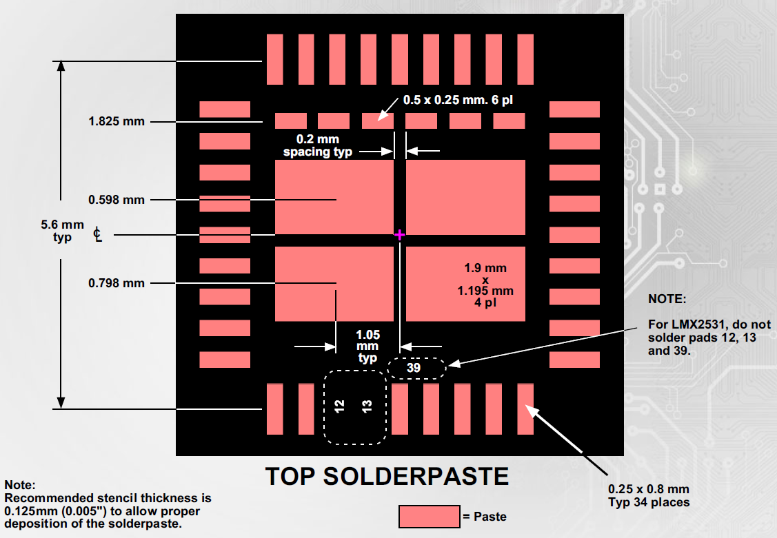
10 Layout
10.1 Layout Guidelines
For the layout of the LMX2531, perhaps the most important factor is to be aware of the package footprint. The asymmetrical land pattern can cause issues if not correctly done.
10.1.1 Typical Connection Diagram
10.1.1.1 VccDIG, VccVCO, VccBUF, and VccPLL
These pins are inputs to voltage regulators. Because the LMX2531 contains internal regulators, the power supply noise rejection is very good and capacitors at this pin are not critical. An RC filter can be used to reduce supply noise, but if the capacitor is too large and is placed too close to these pins, they can sometimes cause phase noise degradation in the 100 — 300 kHz offset range. Recommended values are from open to 1 μF. The 10 Ω series resistors serve to filter power supply noise and isolate these pins from large capacitances.
10.1.1.3 VrefVCO
If the VrefVCO capacitor is changed, it is recommended to keep this capacitor between 1/100 and 1/1000 of the value of the VregVCO capacitor.
10.1.1.4 VregVCO
Because this pin is the output of a regulator, there are stability concerns if there is not sufficient series resistance. For ceramic capacitors, the ESR (Equivalent Series Resistance) is too low, and it is recommended that a series resistance of 1 — 3.3 Ω is necessary. If there is insufficient ESR, then there may be degradation in the phase noise, especially in the 100 — 300 kHz offset. Recommended values are from 1 μF to 10 μF.
10.1.1.5 VregPLL1VregPLL2
The choice of the capacitor value at this pin involves a trade-off between integer spurs and phase noise in the 100 — 300 kHz offset range. Using a series resistor of about 220 mΩ in series with a capacitance that has an impedance of about 150 mΩ at the phase detector frequency seems to give an optimal trade-off. For instance, if the phase detector frequency is 2.5 MHz, then make this series capacitor 470 nF. If the phase detector frequency is 10 MHz, make this capacitance about 100 nF.
10.2 Layout Example