SNAS252S October 2005 – December 2014 LMX2531
PRODUCTION DATA.
- 1 Features
- 2 Applications
- 3 Description
- 4 Revision History
- 5 Pin Configuration and Functions
- 6 Specifications
-
7 Detailed Description
- 7.1 Overview
- 7.2 Functional Block Diagram
- 7.3 Feature Description
- 7.4 Device Functional Modes
- 7.5 Programming
- 7.6
Register Maps
- 7.6.1
General Programming Information
- 7.6.1.1 Initialization Sequence
- 7.6.1.2 Complete Register Content Map
- 7.6.1.3 Register R0
- 7.6.1.4 Register R1
- 7.6.1.5 Register R2
- 7.6.1.6 Register R3
- 7.6.1.7 Register R4
- 7.6.1.8
Register R5
- 7.6.1.8.1 EN_PLL -- Enable Bit for PLL
- 7.6.1.8.2 EN_VCO -- Enable Bit for the VCO
- 7.6.1.8.3 EN_OSC -- Enable Bit for the Oscillator Inverter
- 7.6.1.8.4 EN_VCOLDO -- Enable Bit for the VCO LDO
- 7.6.1.8.5 EN_PLLLDO1 -- Enable Bit for the PLL LDO 1
- 7.6.1.8.6 EN_PLLLDO2 -- Enable Bit for the PLL LDO 2
- 7.6.1.8.7 EN_DIGLDO -- Enable Bit for the digital LDO
- 7.6.1.8.8 REG_RST -- Resets All Registers to Default Settings
- 7.6.1.9
Register R6
- 7.6.1.9.1 C3_C4_ADJ[2:0] -- Value FOR C3 and C4 In The Internal Loop Filter
- 7.6.1.9.2 R3_ADJ_FL[1:0] -- Value for Internal Loop Filter Resistor R3 During Fastlock
- 7.6.1.9.3 R3_ADJ[1:0] -- Value for Internal Loop Filter Resistor R3
- 7.6.1.9.4 R4_ADJ_FL[1:0] -- Value for Internal Loop Filter Resistor R4 During Fastlock
- 7.6.1.9.5 R4_ADJ[1:0] -- Value for Internal Loop Filter Resistor R4
- 7.6.1.9.6 EN_LPFLTR-- Enable for Partially Integrated Internal Loop Filter
- 7.6.1.9.7 VCO_ACI_SEL
- 7.6.1.9.8 XTLSEL[2:0] -- OSCin Select
- 7.6.1.10 Register R7
- 7.6.1.11 Register R8
- 7.6.1.12 Register R9
- 7.6.1.13 Register R12
- 7.6.1
General Programming Information
- 8 Application and Implementation
- 9 Power Supply Recommendations
- 10Layout
- 11Device and Documentation Support
- 12Mechanical, Packaging, and Orderable Information
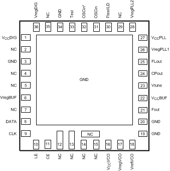
5 Pin Configuration and Functions
NJH0036D Package
36-Pin WQFN, D Version, (LMX2531LQ1146E/1226E/1312E/1415E/1515E/2820E/3010E)
Top View
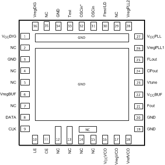
NJG0036A Package
36-Pin WQFN, A Version, (All Other Versions)
Top View
Pin Functions
| PIN | TYPE | DESCRIPTION | |
|---|---|---|---|
| NAME | NO. | ||
| CE | 11 | Input | Chip Enable Input. High impedance CMOS input. This pin must not exceed 2.75 V. When CE is brought high the LMX2531 is powered up corresponding to the internal power control bits. Although the part can be programmed when powered down, it is still necessary to reprogram the R0 register to get the part to re-lock. |
| CLK | 9 | Input | MICROWIRE clock input. High impedance CMOS input. This pin must not exceed 2.75 V. Data is clocked into the shift register on the rising edge. |
| CPout | 24 | Output | Charge pump output for PLL. For connection to Vtune through an external passive loop filter. |
| DATA | 8 | Input | MICROWIRE serial data input. High impedance CMOS input. This pin must not exceed 2.75 V. Data is clocked in MSB first. The last bits clocked in form the control or register select bits. |
| FLout | 25 | Output | An open drain NMOS output which is used for FastLock or a general purpose output. |
| Fout | 21 | Output | Buffered RF Output for the VCO. |
| Ftest/LD | 30 | Output | Multiplexed CMOS output. Typically used to monitor PLL lock condition. |
| GND | 3 | — | Ground |
| GND | 19 | — | Ground for the VCO circuitry. |
| GND | 20 | — | Ground for the VCO Output Buffer circuitry. |
| GND | 34 | — | Ground |
| LE | 10 | Input | MICROWIRE Latch Enable input. High impedance CMOS input. This pin must not exceed 2.75 V. Data stored in the shift register is loaded into the selected latch register when LE goes HIGH. |
| NC | 2, 4, 5, 7, 12, 13, 29, 35 | — | No Connect. |
| NC | 14, 15 | — | No Connect. Do NOT ground. This also includes the pad above these pins. |
| OSCin | 31 | Input | Oscillator input. |
| OSCin* | 32 | Input | Oscillator complimentary input. When a single ended source is used, then a bypass capacitor should be placed as close as possible to this pin and be connected to ground. |
| Test | 33 | Output | This pin is for test purposes and should be grounded for normal operation. |
| VccBUF | 22 | — | Power Supply for the VCO Buffer circuitry. Input may range from 2.8 — 3.2 V. Bypass capacitors should be placed as close as possible to this pin and ground. |
| VccDIG | 1 | — | Power Supply for digital LDO circuitry. Input may range from 2.8 — 3.2 V. Bypass capacitors should be placed as close as possible to this pin and ground. |
| VccPLL | 27 | — | Power Supply for the PLL. Input may range from 2.8 — 3.2 V. Bypass capacitors should be placed as close as possible to this pin and ground. |
| VccVCO | 16 | — | Power Supply for VCO regulator circuitry. Input may range from 2.8 — 3.2 V. Bypass capacitors should be placed as close as possible to this pin and ground. |
| VrefVCO | 18 | — | Internal reference voltage for VCO LDO. Not intended to drive an external load. Connect to ground with a capacitor. |
| VregBUF | 6 | — | Internally regulated voltage for the VCO buffer circuitry. Connect to ground with a capacitor. |
| VregDIG | 36 | — | Internally regulated voltage for LDO digital circuitry. |
| VregPLL1 | 26 | — | Internally regulated voltage for PLL charge pump. Not intended to drive an external load. Connect to ground with a capacitor. |
| VregPLL2 | 28 | — | Internally regulated voltage for RF digital circuitry. Not intended to drive an external load. Connect to ground with a capacitor. |
| VregVCO | 17 | — | Internally regulated voltage for VCO circuitry. Not intended to drive an external load. Connect to ground with a capacitor and some series resistance. |
| Vtune | 23 | Input | Tuning voltage input for the VCO. For connection to the CPout pin through an external passive loop filter. |