SNOSB31J July 2009 – December 2014 LMX2541
PRODUCTION DATA.
- 1 Features
- 2 Applications
- 3 Description
- 4 Revision History
- 5 Device Comparison Table
- 6 Pin Configuration and Functions
- 7 Specifications
- 8 Parameter Measurement Information
-
9 Detailed Description
- 9.1 Overview
- 9.2 Functional Block Diagrams
- 9.3
Feature Description
- 9.3.1 PLL Reference Oscillator Input Pins
- 9.3.2 PLL R Divider
- 9.3.3 PLL Phase Detector and Charge Pump
- 9.3.4 PLL N Divider and Fractional Circuitry
- 9.3.5 Partially Integrated Loop Filter
- 9.3.6 Low Noise, Fully Integrated VCO
- 9.3.7 Programmable VCO Divider
- 9.3.8 Programmable RF Output Buffer
- 9.3.9 Powerdown Modes
- 9.3.10 Fastlock
- 9.3.11 Lock Detect
- 9.3.12 Current Consumption
- 9.3.13 Fractional Spurs
- 9.3.14 Impact of VCO_DIV on Fractional Spurs
- 9.3.15 PLL Phase Noise
- 9.3.16 Impact of Modulator Order, Dithering, and Larger Equivalent Fractions on Spurs and Phase Noise
- 9.3.17 Modulator Order
- 9.3.18 Programmable Output Power with On/Off
- 9.3.19 Loop Filter
- 9.3.20 Internal VCO Digital Calibration Time
- 9.4 Device Functional Modes
- 9.5 Programming
- 9.6
Register Maps
- 9.6.1
Register R7
- 9.6.1.1 Register R13
- 9.6.1.2 Register R12
- 9.6.1.3 Register R9
- 9.6.1.4 Register R8
- 9.6.1.5 Register R6
- 9.6.1.6 Register R5
- 9.6.1.7
Register R4
- 9.6.1.7.1 OSC_FREQ [7:0] -- OSCin Frequency for VCO Calibration Clocking
- 9.6.1.7.2 VCO_DIV[5:0] - VCO Divider
- 9.6.1.7.3 R3_LF[2:0] -- Value for Internal Loop Filter Resistor R3
- 9.6.1.7.4 R4_LF[2:0] -- Value for Internal Loop Filter Resistor R4
- 9.6.1.7.5 C3_LF[3:0] -- Value for C3 in the Internal Loop Filter
- 9.6.1.7.6 C4_LF[3:0] -- Value for C4 in the Internal Loop Filter
- 9.6.1.8
Register R3
- 9.6.1.8.1 MODE[1:0] -- Operational Mode
- 9.6.1.8.2 Powerdown -- Powerdown Bit
- 9.6.1.8.3 XO - Crystal Oscillator Mode Select
- 9.6.1.8.4 CPG[4:0] -- Charge Pump Current
- 9.6.1.8.5 MUX[3:0] -- Multiplexed Output for Ftest/LD Pin
- 9.6.1.8.6 CPP - Charge Pump Polarity
- 9.6.1.8.7 OSC2X-- OSCin Frequency Doubler
- 9.6.1.8.8 FDM - Extended Fractional Denominator Mode Enable
- 9.6.1.8.9 ORDER[2:0] -- Delta-Sigma Modulator Order
- 9.6.1.8.10 DITH[1:0] -- Dithering
- 9.6.1.8.11 CPT - Charge Pump TRI-STATE
- 9.6.1.8.12 DLOCK[2:0] - Controls for Digital Lock Detect
- 9.6.1.8.13 FSK - Frequency Shift Keying
- 9.6.1.9 Register R2
- 9.6.1.10 Registers R1 and R0
- 9.6.1
Register R7
-
10Application and Implementation
- 10.1
Application Information
- 10.1.1 Determining the Best Frequency Option of the LMX2541 to Use
- 10.1.2 RFout Output Power Test Setup
- 10.1.3 Phase Noise Measurement Test Setup
- 10.1.4 Input and Output Impedance Test Setup
- 10.1.5 ExtVCOin (NOT OSCin) Input Sensitivity Test Setup
- 10.1.6 OSCin Input Sensitivity Test Setup
- 10.1.7 Typical Connections
- 10.2 Typical Application
- 10.1
Application Information
- 11Power Supply Recommendations
- 12Layout
- 13Device and Documentation Support
- 14Mechanical, Packaging, and Orderable Information
パッケージ・オプション
デバイスごとのパッケージ図は、PDF版データシートをご参照ください。
メカニカル・データ(パッケージ|ピン)
- NJK|36
サーマルパッド・メカニカル・データ
発注情報
6 Pin Configuration and Functions
NJK Package
36-Pin WQFN
Top View
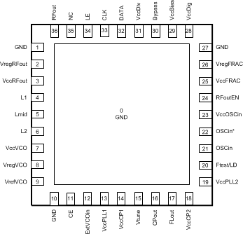
Pin Functions
| PIN | TYPE | DESCRIPTION | |
|---|---|---|---|
| NAME | NO. | ||
| Bypass | 30 | Bypass | Put a cap to the VccBias pin. |
| CE | 11 | CMOS | Chip Enable. The device needs to be programmed for this pin to properly power down the device. |
| CLK | 33 | High-Z Input | MICROWIRE clock input. High impedance CMOS input. This pin is used for the digital FSK modulation feature. |
| CPout | 16 | Output | Charge pump output. |
| DATA | 32 | High-Z Input | MICROWIRE serial data input. High impedance CMOS input. |
| ExtVCOin | 12 | RF Input | Optional input for use with an external VCO. This pin should be AC coupled if used or left open if not used. |
| FLout | 17 | Output | Fastlock output. |
| Ftest/LD | 20 | Output | Software controllable multiplexed CMOS output. Can be used to monitor PLL lock condition. |
| GND | 0 | GND | The DAP pad must be grounded. |
| GND | 1 | GND | |
| GND | 10 | GND | |
| GND | 27 | GND | |
| L1 | 4 | NC | Do not connect this pin. |
| L2 | 6 | NC | Do not connect this pin. |
| LE | 34 | High-Z Input | MICROWIRE Latch Enable input. High impedance CMOS input. |
| Lmid | 5 | NC | Do not connect this pin. |
| NC | 35 | NC | No connect. |
| OSCin | 21 | High-Z Input | Oscillator input signal. If not being used with an external crystal, this input should be AC coupled. |
| OSCin* | 22 | High-Z Input | Complementary oscillator input signal. Can also be used with an external crystal. If not being used with an external crystal, this input should be AC coupled. |
| RFout | 36 | RF Output | RF output. Must be AC coupled if used. |
| RFoutEN | 24 | Input | Software programmable output enable pin. |
| VccBias | 29 | Supply | Supply for Bias circuitry that is for the whole chip. |
| VccCP1 | 14 | Supply | Power supply for PLL charge pump. |
| VccCP2 | 18 | Supply | Power supply for PLL charge pump. |
| VccDig | 28 | Supply | Supply for digital circuitry, such the MICROWIRE. |
| VccDiv | 31 | Supply | Supply for the output divider |
| VccFRAC | 25 | Supply (LDO Input) |
Power Supply for the PLL fractional circuitry. |
| VccOSCin | 23 | Supply | Supply for the OSCin buffer. |
| VccPLL1 | 13 | Supply | Power supply for PLL. |
| VccPLL2 | 19 | Supply | Power supply for PLL. |
| VccRFout | 3 | Supply (LDO Input) |
Supply for the RF output buffer. |
| VccVCO | 7 | Supply (LDO Input) |
Supply for the VCO. |
| VregFRAC | 26 | LDO Output | Regulated power supply used for the fractional delta-sigma circuitry. |
| VregRFout | 2 | LDO Output | LDO Output for RF output buffer. |
| VrefVCO | 9 | LDO Bypass | LDO Bypass |
| VregVCO | 8 | LDO Output | LDO Output for VCO |
| Vtune | 15 | High-Z Input | Tuning voltage input to the VCO. |