SNOSB31J July 2009 – December 2014 LMX2541
PRODUCTION DATA.
- 1 Features
- 2 Applications
- 3 Description
- 4 Revision History
- 5 Device Comparison Table
- 6 Pin Configuration and Functions
- 7 Specifications
- 8 Parameter Measurement Information
-
9 Detailed Description
- 9.1 Overview
- 9.2 Functional Block Diagrams
- 9.3
Feature Description
- 9.3.1 PLL Reference Oscillator Input Pins
- 9.3.2 PLL R Divider
- 9.3.3 PLL Phase Detector and Charge Pump
- 9.3.4 PLL N Divider and Fractional Circuitry
- 9.3.5 Partially Integrated Loop Filter
- 9.3.6 Low Noise, Fully Integrated VCO
- 9.3.7 Programmable VCO Divider
- 9.3.8 Programmable RF Output Buffer
- 9.3.9 Powerdown Modes
- 9.3.10 Fastlock
- 9.3.11 Lock Detect
- 9.3.12 Current Consumption
- 9.3.13 Fractional Spurs
- 9.3.14 Impact of VCO_DIV on Fractional Spurs
- 9.3.15 PLL Phase Noise
- 9.3.16 Impact of Modulator Order, Dithering, and Larger Equivalent Fractions on Spurs and Phase Noise
- 9.3.17 Modulator Order
- 9.3.18 Programmable Output Power with On/Off
- 9.3.19 Loop Filter
- 9.3.20 Internal VCO Digital Calibration Time
- 9.4 Device Functional Modes
- 9.5 Programming
- 9.6
Register Maps
- 9.6.1
Register R7
- 9.6.1.1 Register R13
- 9.6.1.2 Register R12
- 9.6.1.3 Register R9
- 9.6.1.4 Register R8
- 9.6.1.5 Register R6
- 9.6.1.6 Register R5
- 9.6.1.7
Register R4
- 9.6.1.7.1 OSC_FREQ [7:0] -- OSCin Frequency for VCO Calibration Clocking
- 9.6.1.7.2 VCO_DIV[5:0] - VCO Divider
- 9.6.1.7.3 R3_LF[2:0] -- Value for Internal Loop Filter Resistor R3
- 9.6.1.7.4 R4_LF[2:0] -- Value for Internal Loop Filter Resistor R4
- 9.6.1.7.5 C3_LF[3:0] -- Value for C3 in the Internal Loop Filter
- 9.6.1.7.6 C4_LF[3:0] -- Value for C4 in the Internal Loop Filter
- 9.6.1.8
Register R3
- 9.6.1.8.1 MODE[1:0] -- Operational Mode
- 9.6.1.8.2 Powerdown -- Powerdown Bit
- 9.6.1.8.3 XO - Crystal Oscillator Mode Select
- 9.6.1.8.4 CPG[4:0] -- Charge Pump Current
- 9.6.1.8.5 MUX[3:0] -- Multiplexed Output for Ftest/LD Pin
- 9.6.1.8.6 CPP - Charge Pump Polarity
- 9.6.1.8.7 OSC2X-- OSCin Frequency Doubler
- 9.6.1.8.8 FDM - Extended Fractional Denominator Mode Enable
- 9.6.1.8.9 ORDER[2:0] -- Delta-Sigma Modulator Order
- 9.6.1.8.10 DITH[1:0] -- Dithering
- 9.6.1.8.11 CPT - Charge Pump TRI-STATE
- 9.6.1.8.12 DLOCK[2:0] - Controls for Digital Lock Detect
- 9.6.1.8.13 FSK - Frequency Shift Keying
- 9.6.1.9 Register R2
- 9.6.1.10 Registers R1 and R0
- 9.6.1
Register R7
-
10Application and Implementation
- 10.1
Application Information
- 10.1.1 Determining the Best Frequency Option of the LMX2541 to Use
- 10.1.2 RFout Output Power Test Setup
- 10.1.3 Phase Noise Measurement Test Setup
- 10.1.4 Input and Output Impedance Test Setup
- 10.1.5 ExtVCOin (NOT OSCin) Input Sensitivity Test Setup
- 10.1.6 OSCin Input Sensitivity Test Setup
- 10.1.7 Typical Connections
- 10.2 Typical Application
- 10.1
Application Information
- 11Power Supply Recommendations
- 12Layout
- 13Device and Documentation Support
- 14Mechanical, Packaging, and Orderable Information
パッケージ・オプション
デバイスごとのパッケージ図は、PDF版データシートをご参照ください。
メカニカル・データ(パッケージ|ピン)
- NJK|36
サーマルパッド・メカニカル・データ
発注情報
7 Specifications
7.1 Absolute Maximum Ratings
over operating free-air temperature range (unless otherwise noted) (1)(2)| MIN | MAX | UNIT | ||
|---|---|---|---|---|
| Vcc | Power Supply Voltage | –0.3 | 3.6 | V |
| VIN | Input Voltage to pins other than Vcc Pins (3) |
–0.3 | (Vcc + 0.3) | V |
| TL | Lead Temperature (solder 4 sec.) | 260 | °C | |
| Tstg | Storage Temperature | –65 | 150 | °C |
7.2 ESD Ratings
| VALUE | UNIT | |||
|---|---|---|---|---|
| V(ESD) | Electrostatic discharge | Human body model (HBM), per ANSI/ESDA/JEDEC JS-001(1) | ±2500 | V |
| Charged-device model (CDM), per JEDEC specification JESD22-C101(2) | ±1750 | |||
| Machine model (MM) | ±400 | |||
7.3 Recommended Operating Conditions
| MIN | NOM | MAX | UNIT | ||
|---|---|---|---|---|---|
| Vcc | Power Supply Voltage (All Vcc Pins) | 3.15 | 3.3 | 3.45 | V |
| TA | Ambient Temperature | –40 | 85 | °C | |
7.4 Thermal Information
| THERMAL METRIC(1) | LMX2541 SQ2060E |
LMX2541 SQ2060E |
LMX2541 SQ2060E |
UNIT | |
|---|---|---|---|---|---|
| 9 Thermal Vias(2) | 13 Thermal Vias(3) | 16 Thermal Vias(4) | |||
| RθJA | Junction-to-ambient thermal resistance | 31.7 | 30.3 | 29.8 | °C/W |
| ψJT | Junction-to-top characterization parameter | 7.3 | 7.3 | 7.3 | |
7.5 Electrical Characteristics
(3.15 V ≤ VCC ≤ 3.45 V, -40°C ≤ TA ≤ 85 °C; except as specified. Typical values are at Vcc = 3.3 V, 25 C.)| PARAMETER | TEST CONDITIONS | MIN | TYP | MAX | UNIT | ||||
|---|---|---|---|---|---|---|---|---|---|
| CURRENT CONSUMPTION | |||||||||
| ICC | Entire Chip Supply Current with all blocks enabled | Default Power Mode (1) |
VCO_DIV>1 | 170 | 204 | mA | |||
| VCO_DIV=1 | 130 | 156 | |||||||
| IPLL | Current for External VCO Mode | RFoutEN = LOW | 72 | 94 | mA | ||||
| IDIV | Current for Divider Only Mode | VCO_DIV >1 Default Power Mode (1) |
84 | 110 | mA | ||||
| ICCPD | Power Down Current | CE = 0 V, Device Initialized | 100 | 250 | µA | ||||
| OSCILLATOR (NORMAL MODE OPERATION WITH XO=0) | |||||||||
| IIHOSC in | Oscillator Input High Current for OSCin and OSCin* | VIH = 2.75 V | 300 | µA | |||||
| IILOSCin | Oscillator Input Low Current for OSCin and OSCin* pins | VIL = 0 | –100 | µA | |||||
| fOSCin | OSCin Frequency Range (2) |
OSC_2X = 1 | 5 | 52 | MHz | ||||
| OSC_2X = 0 | MODE = 0 | 5 | 700 | ||||||
| MODE = 1 | 5 | 900 | |||||||
| dvOSCin | Slew Rate | (2) | 150 | V/µs | |||||
| vOSCin | Oscillator Sensitivity | dvOSCin ≥ 150 V/µs | Single-Ended | 0.2 | 2.0 | Vpp | |||
| Differential | 0.4 | 3.1 | |||||||
| OSCILLATOR (CRYSTAL MODE WITH XO=1) | |||||||||
| fXTAL | Crystal Frequency Range | VIH = 2.75 V | 5 | 20 | MHz | ||||
| ESRXTAL | Crystal Equivalent Series Resistance | This a requirement for the crystal, not a characteristic of the LMX2541. | 100 | Ω | |||||
| PXTAL | Power Dissipation in Crystal | This requirement is for the crystal, not a characteristic of the LMX2541. | 200 | µW | |||||
| COSCin | Input Capacitance of OSCin | 6 | pF | ||||||
| PLL | |||||||||
| fPD | Phase Detector Frequency | 104 | MHz | ||||||
| ICPout | Charge Pump Output Current Magnitude |
CPG = 1X | 100 | µA | |||||
| CPG = 2X | 200 | ||||||||
| CPG = 3X | 300 | ||||||||
| ... | ... | ||||||||
| CPG=32X | 3200 | ||||||||
| ICPoutTRI | CP TRI-STATE Current | 0.4 V < VCPout < Vcc - 0.4 | 1 | 5 | nA | ||||
| ICPoutMM | Charge Pump Sink vs. Source Mismatch |
VCPout = Vcc / 2 TA = 25°C |
3% | 10% | |||||
| ICPoutV | Charge Pump Current vs. CP Voltage Variation |
0.4 V < VCPout < Vcc - 0.4 TA = 25°C |
4% | ||||||
| ICPoutT | CP Current vs. Temperature Variation | VCPout = Vcc / 2 | 8% | ||||||
| LN(f) (3) |
Normalized PLL 1/f Noise LNPLL_flicker(10 kHz) |
CPG = 1X | –116 | dBc/Hz | |||||
| CPG = 32X | –124.5 | ||||||||
| Normalized PLL Noise Floor LNPLL_flat(1 Hz) |
CPG = 1X | –220.8 | dBc/Hz | ||||||
| CPG = 32X | –225.4 | ||||||||
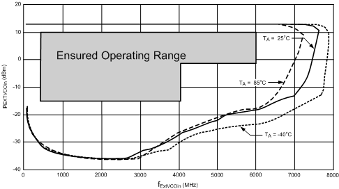
| fExtVCOin | PLL Input Frequency | RFout Buffer Enabled and VCO_DIV > 1 | 400 | 4000 | MHz | ||||
| RFout Buffer Disabled and VCO_DIV = 1 | 400 | 6000 | |||||||
| pExtVCOin | PLL Input Sensitivity ((2) applies to Max Limit Only) |
fExtVCOin ≤ 4 GHz | –15 | 10 | dBm | ||||
| fExtVCOin > 4 GHz | –5 | 10 | |||||||
| VCO SPECIFICATIONS | |||||||||
| fVCO | Internal VCO Frequency Range | Mode = Full Chip Mode This is the frequency before the VCO divider. |
2060E | 1990 | 2240 | MHz | |||
| 2380E | 2200 | 2530 | |||||||
| 2690E | 2490 | 2865 | |||||||
| 3030E | 2810 | 3230 | |||||||
| 3320E | 3130 | 3600 | |||||||
| 3740E | 3480 | 4000 | |||||||
| ΔTCL | Maximum Allowable Temperature Drift for Continuous Lock | (2),(4) | 125 | °C | |||||
| pRFout | RF Output Power |
Maximum Frequency Default Power Mode VCO_DIV=1 |
2060E | 3.5 | dBm | ||||
| 2380E | 2.8 | ||||||||
| 2690E | 1.6 | ||||||||
| 3030E | 1.2 | ||||||||
| 3320E | 0.2 | ||||||||
| 3740E | –0.3 | ||||||||
| ΔPRFout | Change in Output Power | Fixed Temperature with 100 MHz frequency change at the output | 0.3 | dB | |||||
| Fixed frequency with a change over the entire temperature range | 0.4 | ||||||||
| KVtune | Fine Tuning Sensitivity | The lower number in the range applies when the VCO is at its lowest frequency and the higher number applies when the VCO is at its highest frequency. A linear approximation can be used for frequencies between these two cases. | 2060E | 13 - 23 | MHz/V | ||||
| 2380E | 16 - 30 | ||||||||
| 2690E | 17 - 32 | ||||||||
| 3030E | 20 - 37 | ||||||||
| 3320E | 21 - 37 | ||||||||
| 3740E | 24 - 42 | ||||||||
| HSRFout | Second Harmonic (6) |
Default Power Mode (1) 50 Ω Load |
VCO_DIV = 2 | –20 | dBc | ||||
| VCO_DIV = 3 | –20 | ||||||||
| DERFout | Duty Cycle Error (6) |
Default Power Mode (1) 50 Ω Load |
VCO_DIV = 2 | 3% | |||||
| VCO_DIV = 3 | 3% | ||||||||
| PSHVCO | VCO Frequency Pushing | CVregVCO = 4.7 µF, Open Loop | 600 | kHz/V | |||||
| PULVCO | VCO Frequency Pulling | VSWR 1.7 to 1 (6 dB Pad) |
VCO_DIV = 1 | ±800 | kHz | ||||
| VCO_DIV > 1 | ±60 | ||||||||
| σΦ | RMS Phase Error | Integration Bandwidth = 100 Hz to 20 MHz Middle VCO Frequency 100 MHz Wenzel Crystal Reference Integer Mode Optimized Loop Bandwidth |
2060E | 1.6 | mRad | ||||
| 2380E | 1.8 | ||||||||
| 2690E | 2.1 | ||||||||
| 3030E | 2.1 | ||||||||
| 3320E | 2.3 | ||||||||
| 3740E | 2.6 | ||||||||
| VCO PHASE NOISE(5) | |||||||||
| L(f)Fout | Phase Noise 2060E |
fRFout = Min VCO Frequency |
10-kHz Offset | –89.7 | dBc/Hz | ||||
| 100-kHz Offset | –113.7 | ||||||||
| 1-MHz Offset | –134.9 | ||||||||
| 10-MHz Offset | –155.4 | ||||||||
| 20-MHz Offset | –160.3 | ||||||||
| fRFout = Max VCO Frequency |
10-kHz Offset | –86.5 | |||||||
| 100-kHz Offset | –111.4 | ||||||||
| 1-MHz Offset | –132.8 | ||||||||
| 10-MHz Offset | –153.4 | ||||||||
| 20-MHz Offset | –158.5 | ||||||||
| L(f)Fout | Phase Noise 2380E |
fRFout = Min VCO Frequency |
10-kHz Offset | –87.9 | dBc/Hz | ||||
| 100-kHz Offset | –112.7 | ||||||||
| 1-MHz Offset | –133.8 | ||||||||
| 10-MHz Offset | –154.2 | ||||||||
| 20-MHz Offset | –159.5 | ||||||||
| fRFout = Max VCO Frequency |
10-kHz Offset | –83.4 | |||||||
| 100-kHz Offset | –109.1 | ||||||||
| 1-MHz Offset | –130.8 | ||||||||
| 10-MHz Offset | –151.8 | ||||||||
| 20-MHz Offset | –157.5 | ||||||||
| L(f)Fout | Phase Noise 2690E |
fRFout = Min VCO Frequency |
10-kHz Offset | –86.9 | dBc/Hz | ||||
| 100-kHz Offset | –111.8 | ||||||||
| 1-MHz Offset | –133.3 | ||||||||
| 10-MHz Offset | –154.2 | ||||||||
| 20-MHz Offset | –159.4 | ||||||||
| fRFout = Max VCO Frequency |
10-kHz Offset | –82.3 | |||||||
| 100-kHz Offset | –108.4 | ||||||||
| 1-MHz Offset | –130.3 | ||||||||
| 10-MHz Offset | –151.1 | ||||||||
| 20-MHz Offset | –156.7 | ||||||||
| L(f)Fout | Phase Noise 3030E |
fRFout = Min VCO Frequency |
10-kHz Offset | –86.1 | dBc/Hz | ||||
| 100-kHz Offset | –110.5 | ||||||||
| 1-MHz Offset | –132.0 | ||||||||
| 10-MHz Offset | –152.2 | ||||||||
| 20-MHz Offset | –157.1 | ||||||||
| fRFout = Max VCO Frequency |
10-kHz Offset | –82.2 | |||||||
| 100-kHz Offset | –107.7 | ||||||||
| 1-MHz Offset | –129.4 | ||||||||
| 10-MHz Offset | –150.5 | ||||||||
| 20-MHz Offset | –156.1 | ||||||||
| L(f)Fout | Phase Noise 3320E |
fRFout = Min VCO Frequency |
10-kHz Offset | –84.1 | dBc/Hz | ||||
| 100-kHz Offset | –109.1 | ||||||||
| 1-MHz Offset | –130.7 | ||||||||
| 10-MHz Offset | –151.6 | ||||||||
| 20-MHz Offset | –156.9 | ||||||||
| fRFout = Max VCO Frequency |
10-kHz Offset | –82.0 | |||||||
| 100-kHz Offset | –107.0 | ||||||||
| 1-MHz Offset | –128.5 | ||||||||
| 10-MHz Offset | –149.6 | ||||||||
| 20-MHz Offset | –155.2 | ||||||||
| L(f)Fout | Phase Noise 3740E |
fRFout = Min VCO Frequency |
10-kHz Offset | –83.9 | dBc/Hz | ||||
| 100-kHz Offset | –108.3 | ||||||||
| 1-MHz Offset | –129.9 | ||||||||
| 10-MHz offset | –150.6 | ||||||||
| 20-MHz Offset | –156.5 | ||||||||
| fRFout = Max VCO Frequency |
10-kHz Offset | –81.6 | |||||||
| 100-kHz Offset | –106.5 | ||||||||
| 1-MHz Offset | –127.7 | ||||||||
| 10-MHz Offset | –148.6 | ||||||||
| 20-MHz Offset | –154.2 | ||||||||
| DIGITAL INTERFACE (DATA, CLK, LE, CE, Ftest/LD, FLout,RFoutEN) | |||||||||
| VIH | High-Level Input Voltage | 1.6 | Vcc | V | |||||
| VIL | Low-Level Input Voltage | 0.4 | V | ||||||
| IIH | High-Level Input Current | VIH = 1.75, XO = 0 | –5 | 5 | µA | ||||
| IIL | Low-Level Input Current | VIL = 0 V , XO = 0 | –5 | 5 | µA | ||||
| VOH | High-Level Output Voltage | IOH = 500 µA | 2 | V | |||||
| VOL | Low-Level Output Voltage | IOL = -500 µA | 0 | 0.4 | V | ||||
| ILeak | Leakage Current | Ftest/LD and FLout Pins Only | –5 | 5 | µA | ||||
7.6 Timing Requirements
| MIN | NOM | MAX | UNIT | |||
|---|---|---|---|---|---|---|
| tCE | Clock to Enable Low Time | See Figure 1 | 25 | ns | ||
| tCS | Data to Clock Set Up Time | See Figure 1 | 25 | ns | ||
| tCH | Data to Clock Hold Time | See Figure 1 | 20 | ns | ||
| tCWH | Clock Pulse Width High | See Figure 1 | 25 | ns | ||
| tCWL | Clock Pulse Width Low | See Figure 1 | 25 | ns | ||
| tCES | Enable to Clock Set Up Time | See Figure 1 | 25 | ns | ||
| tEWH | Enable Pulse Width High | See Figure 1 | 25 | ns | ||
 Figure 1. Serial Data Timing Diagram
7.7 Typical Characteristics
7.7.1 Not Ensured Characteristics
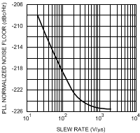 Figure 2. PLL Normalized Noise Floor vs OSCin Slew Rate (KPD = 32X)
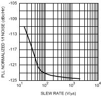 Figure 4. PLL Normalized 1/f Noise vs OSCin Slew Rate (KPD = 32X)
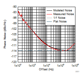 Figure 6. PLL 1/f and Noise Floor Measurement of the LMX2541SQ3740E
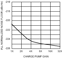 Figure 3. PLL Normalized Noise Floor vs Charge Pump Gain (Slew Rate = 2000 V/μs)
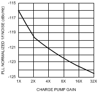 Figure 5. PLL Normalized 1/f Noise vs Charge Pump Gain (Slew Rate = 2000 V/μs)
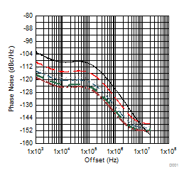
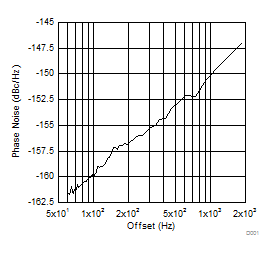
Table 1. Relative VCO Phase Noise Over Temperature Drift
(AC_TEMP_COMP = 24, Vcc = 3.3 V)(1)
| TEMPERATURE | PHASE NOISE CHANGE IN CELSIUS FOR VARIOUS OFFSETS | |||||
|---|---|---|---|---|---|---|
| LOCK | CURRENT | 10 kHz | 100 kHz | 1 MHz | 10 MHz | 20 MHz |
| –40 | –40 | +0.4 | –2.0 | –1.6 | –1.8 | –1.6 |
| –40 | 25 | +0.3 | +0.5 | +0.5 | +0.5 | +0.4 |
| –40 | 85 | +0.9 | +2.0 | +2.4 | +2.5 | +2.3 |
| 25 | –40 | +0.2 | –2.2 | –1.7 | –2.0 | –1.8 |
| 25 | 25 | This is the default condition to which these other numbers are normalized to. | ||||
| 25 | 85 | +0.6 | +1.5 | +2.0 | +2.0 | +1.9 |
| 85 | –40 | +0.2 | –2.2 | –1.7 | –1.9 | –1.8 |
| 85 | 25 | +0.2 | +0.2 | +0.3 | +0.2 | +0.2 |
| 85 | 85 | +0.6 | +1.8 | +2.2 | +2.3 | +2.1 |
7.7.2 Output Power in Bypass Mode
The following plots show the trends in output power as a function of temperature, voltage, and frequency. For states where VCOGAIN and OUTTERM are not 12, the table below shows how the output power is modified based on these programmable settings. The measurement of the output power is sensitive to the test circuit. All the numbers in the electrical specifications and typical performance curves were obtained from a characterization setup that accommodate temperature testing and changing of parts. In a more optimized setup the measured RF output power is typically on the order of 1.5 to 2.4 dB higher.
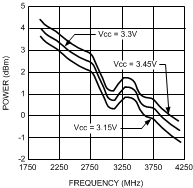 Figure 9. Output Power vs Voltage (VCO_DIV = 1, VCOGAIN = 12, OUTTERM = 12, TA = 25°C)
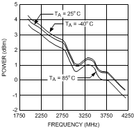 Figure 11. Output Power vs Temperature (VCO_DIV = 1, VCOGAIN = 12, OUTTERM = 12, Vcc = 3.3 V)
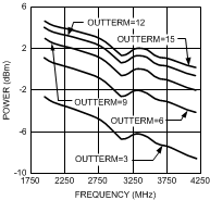 Figure 10. Output Power vs OUTTERM and FREQUENCY (VCO_DIV = 1, TA = 25 °C, Vcc = 3.3 V, VCOGAIN = 12)
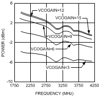 Figure 12. Output Power vs VCOGAIN and FREQUENCY (VCO_DIV = 1, TA = 25 °C, Vcc = 3.3 V, OUTTERM = 12)
Table 2. Change in Output Power in Bypass Mode as a Function of VCOGAIN and OUTTERM
| VCOGAIN | ||||||
|---|---|---|---|---|---|---|
| 3 | 6 | 9 | 12 | 15 | ||
| OUTTERM | 3 | –9.7 | –8.4 | –7.9 | –7.8 | –7.9 |
| 6 | –6.6 | –4.5 | –3.6 | –3.4 | –3.6 | |
| 9 | –5.7 | –3.1 | –1.7 | –1.3 | –1.3 | |
| 12 | –5.4 | –2.5 | –0.8 | +0.0 | +0.1 | |
| 15 | –5.3 | –2.2 | –0.3 | +0.8 | +1.1 | |
7.7.3 Output Power in Divided Mode
The measurement of the output power is sensitive to the test circuit. All the numbers in the electrical specifications and typical performance curves were obtained from a characterization setup that accommodate temperature testing and changing of parts. In a more optimized setup the measured RF output power is typically on the order of 1.5 to 2.4 dB higher.
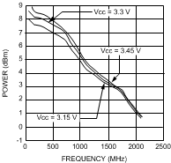
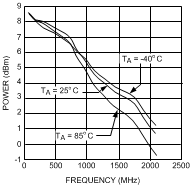
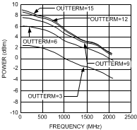
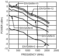
Table 3. Change in Output Power in Divided Mode as a Function of DIVGAIN and OUTTERM(1)
| DIVGAIN | ||||||
|---|---|---|---|---|---|---|
| 3 | 6 | 9 | 12 | 15 | ||
| OUTTERM | 3 | –10.2 | –6.1 | –5.7 | –5.5 | –5.5 |
| 6 | –9.8 | –4.4 | –2.4 | –2.1 | –2.0 | |
| 9 | –9.8 | –4.3 | –1.5 | –0.7 | –0.5 | |
| 12 | –9.9 | –4.3 | –1.4 | +0.0 | +0.2 | |
| 15 | –9.9 | –4.4 | –1.4 | +0.3 | +0.7 | |
7.7.4 RFout Output Impedance
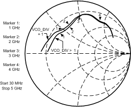
Table 4. RFout Output Impedance vs. VCOGAIN (Bypass Mode)(1)
| Freq. (MHz) | VCOGAIN=3 | VCOGAIN=6 | VCOGAIN=9 | VCOGAIN=12 | VCOGAIN=15 | |||||
|---|---|---|---|---|---|---|---|---|---|---|
| REAL | IMAGINARY | REAL | IMAGINARY | REAL | IMAGINARY | REAL | IMAGINARY | REAL | IMAGINARY | |
| 50 | 3.8 | 2.1 | 5.5 | 1.9 | 7.3 | 1.8 | 9.5 | 1.7 | 10.1 | 1.7 |
| 100 | 4.8 | 4.1 | 6.1 | 3.9 | 7.8 | 3.7 | 9.8 | 3.6 | 10.3 | 3.6 |
| 200 | 5.4 | 5.7 | 6.8 | 6.0 | 8.7 | 6.3 | 10.9 | 6.5 | 11.4 | 6.6 |
| 400 | 5.5 | 9.4 | 7.5 | 10.0 | 9.8 | 10.6 | 12.4 | 11.0 | 13.1 | 11.0 |
| 600 | 5.8 | 15.1 | 8.1 | 15.4 | 10.7 | 15.7 | 13.7 | 15.7 | 14.5 | 15.6 |
| 800 | 7.0 | 20.7 | 9.6 | 20.8 | 12.6 | 20.8 | 15.8 | 20.3 | 16.7 | 20.1 |
| 1000 | 9.2 | 26.3 | 12.1 | 26.1 | 15.4 | 25.6 | 19.0 | 24.6 | 19.8 | 24.1 |
| 1200 | 10.7 | 28.6 | 13.4 | 27.9 | 16.3 | 26.9 | 19.3 | 25.5 | 20.0 | 25.0 |
| 1400 | 12.2 | 30.9 | 14.7 | 29.7 | 17.1 | 28.2 | 19.7 | 26.4 | 20.2 | 25.9 |
| 1600 | 13.7 | 33.2 | 15.9 | 31.5 | 18.0 | 29.5 | 20.1 | 27.4 | 20.5 | 26.8 |
| 1800 | 15.2 | 35.5 | 17.2 | 33.3 | 18.8 | 30.8 | 20.5 | 28.3 | 20.7 | 27.7 |
| 2000 | 14.5 | 39.5 | 16.4 | 37.4 | 17.9 | 35.0 | 19.6 | 32.5 | 19.8 | 31.9 |
| 2200 | 15.6 | 42.9 | 17.4 | 40.7 | 18.7 | 38.2 | 20.3 | 35.6 | 20.4 | 35.0 |
| 2400 | 14.2 | 47.6 | 16.0 | 45.3 | 17.4 | 42.8 | 19.0 | 40.1 | 19.2 | 39.4 |
| 2600 | 12.2 | 51.3 | 14.1 | 48.7 | 15.6 | 46.5 | 17.2 | 43.5 | 17.3 | 42.5 |
| 2800 | 11.5 | 57.9 | 13.7 | 55.3 | 15.3 | 52.4 | 17.0 | 49.0 | 17.1 | 48.3 |
| 3000 | 10.6 | 67.1 | 13.1 | 64.0 | 14.8 | 60.5 | 16.3 | 56.5 | 16.4 | 55.7 |
| 3200 | 13.1 | 77.3 | 15.7 | 73.2 | 17.3 | 69.0 | 18.4 | 64.2 | 18.4 | 63.3 |
| 3400 | 17.6 | 88.1 | 20.0 | 82.8 | 21.1 | 77.4 | 21.7 | 71.8 | 21.5 | 70.8 |
| 3600 | 29.0 | 96.0 | 30.6 | 90.2 | 30.9 | 83.6 | 30.2 | 76.7 | 29.8 | 75.6 |
| 3800 | 38.2 | 99.4 | 38.0 | 94.4 | 36.4 | 87.3 | 34.1 | 80.5 | 33.4 | 79.4 |
| 4000 | 43.5 | 106.0 | 41.6 | 99.0 | 38.9 | 92.0 | 35.5 | 85.1 | 34.8 | 83.7 |
| 4200 | 48.0 | 119.3 | 45.9 | 109.8 | 43.1 | 101.9 | 37.2 | 94.2 | 36.0 | 93.0 |
| 4400 | 62.4 | 137.9 | 56.4 | 126.6 | 49.8 | 117.6 | 42.3 | 109.5 | 40.8 | 108.3 |
| 4600 | 87.0 | 149.4 | 76.0 | 138.1 | 65.4 | 129.5 | 54.3 | 122.2 | 52.3 | 121.2 |
| 4800 | 128.1 | 153.7 | 109.7 | 145.6 | 93.0 | 140.1 | 76.7 | 135.9 | 74.0 | 135.5 |
| 5000 | 168.1 | 134.7 | 145.4 | 135.5 | 124.9 | 138.0 | 105.4 | 141.1 | 102.4 | 141.9 |
Table 5. RFout Output Impedance vs. OUTTERM (Bypass Mode)(1)
| Freq. (MHz) | OUTTERM=3 | OUTTERM=6 | OUTTERM=9 | OUTTERM=12 | TERM=15 | |||||
|---|---|---|---|---|---|---|---|---|---|---|
| REAL | IMAGINARY | REAL | IMAGINARY | REAL | IMAGINARY | REAL | IMAGINARY | REAL | IMAGINARY | |
| 50 | 27.9 | 1.6 | 16.2 | 1.9 | 12.3 | 1.8 | 9.5 | 1.7 | 7.8 | 1.7 |
| 100 | 28.5 | 2.8 | 16.7 | 3.6 | 12.7 | 3.6 | 9.8 | 3.6 | 8.0 | 3.5 |
| 200 | 29.2 | 3.8 | 18.1 | 5.9 | 14.0 | 6.3 | 10.9 | 6.5 | 9.0 | 6.6 |
| 400 | 28.8 | 5.7 | 19.2 | 9.5 | 15.3 | 10.3 | 12.4 | 11.0 | 10.6 | 11.2 |
| 600 | 28.8 | 8.8 | 20.4 | 13.7 | 16.5 | 14.9 | 13.7 | 15.7 | 11.9 | 16.0 |
| 800 | 29.1 | 11.7 | 22.5 | 17.5 | 18.7 | 19.2 | 15.8 | 20.3 | 14.0 | 20.8 |
| 1000 | 28.6 | 13.4 | 22.8 | 19.2 | 19.3 | 21.2 | 16.5 | 22.5 | 14.6 | 23.1 |
| 1200 | 28.0 | 15.0 | 23.1 | 20.9 | 19.8 | 23.2 | 17.1 | 24.7 | 15.2 | 25.4 |
| 1400 | 27.5 | 16.7 | 23.3 | 22.7 | 20.4 | 25.2 | 17.7 | 26.9 | 15.8 | 27.7 |
| 1600 | 27.0 | 18.4 | 23.6 | 24.4 | 20.9 | 27.2 | 18.4 | 29.0 | 16.5 | 30.0 |
| 1800 | 26.4 | 20.1 | 23.9 | 26.1 | 21.4 | 29.2 | 19.0 | 31.2 | 17.1 | 32.3 |
| 2000 | 25.9 | 21.8 | 24.1 | 27.9 | 22.0 | 31.1 | 19.6 | 33.4 | 17.7 | 34.6 |
| 2200 | 25.3 | 23.5 | 24.4 | 29.6 | 22.5 | 33.1 | 20.3 | 35.6 | 18.3 | 36.9 |
| 2400 | 23.1 | 26.9 | 22.9 | 33.2 | 21.3 | 37.1 | 19.0 | 40.1 | 17.0 | 41.8 |
| 2600 | 20.1 | 29.3 | 20.5 | 35.4 | 19.3 | 39.6 | 17.2 | 42.9 | 15.1 | 44.9 |
| 2800 | 18.5 | 34.2 | 19.6 | 40.4 | 18.8 | 45.0 | 17.0 | 49.0 | 14.8 | 51.6 |
| 3000 | 16.6 | 40.6 | 18.1 | 46.9 | 17.8 | 51.9 | 16.3 | 56.5 | 14.3 | 59.7 |
| 3200 | 16.5 | 47.0 | 18.9 | 53.4 | 19.3 | 58.9 | 18.4 | 64.2 | 16.7 | 68.2 |
| 3400 | 17.1 | 53.8 | 20.4 | 60.1 | 21.8 | 65.8 | 21.7 | 71.8 | 20.4 | 76.6 |
| 3600 | 20.8 | 59.4 | 25.4 | 65.0 | 28.3 | 70.5 | 30.2 | 76.8 | 30.3 | 82.5 |
| 3800 | 22.0 | 64.9 | 27.3 | 69.7 | 31.1 | 74.6 | 34.1 | 80.5 | 35.4 | 86.1 |
| 4000 | 23.0 | 70.0 | 28.1 | 74.9 | 32.1 | 80.0 | 35.5 | 86.4 | 37.6 | 92.0 |
| 4200 | 23.7 | 77.9 | 28.6 | 82.8 | 32.8 | 87.7 | 37.0 | 94.2 | 39.9 | 100.9 |
| 4400 | 23.7 | 93.2 | 30.1 | 98.0 | 35.4 | 102.9 | 42.3 | 109.4 | 47.8 | 116.6 |
| 4600 | 27.3 | 107.4 | 36.6 | 112.0 | 44.8 | 116.3 | 54.3 | 122.2 | 62.6 | 128.9 |
| 4800 | 40.1 | 126.6 | 52.2 | 129.8 | 63.3 | 132.3 | 76.7 | 135.9 | 89.3 | 140.5 |
| 5000 | 61.4 | 142.8 | 76.2 | 143.3 | 89.5 | 142.3 | 105.5 | 141.0 | 121.0 | 140.5 |
Table 6. RFout Output Impedance vs. DIVGAIN (Divided Mode)(1)
| Freq. (MHz) | DIVGAIN=3 | DIVGAIN=6 | DIVGAIN=9 | DIVGAIN=12 | DIVGAIN=15 | |||||
|---|---|---|---|---|---|---|---|---|---|---|
| REAL | IMAGINARY | REAL | IMAGINARY | REAL | IMAGINARY | REAL | IMAGINARY | REAL | IMAGINARY | |
| 50 | 3.2 | 2.2 | 3.6 | 2.1 | 5.8 | 2.0 | 13.9 | 1.9 | 22.3 | 1.6 |
| 100 | 4.5 | 4.1 | 4.6 | 4.0 | 6.6 | 3.8 | 14.7 | 3.2 | 23.2 | 2.3 |
| 200 | 5.7 | 5.3 | 6.4 | 5.7 | 7.0 | 5.9 | 15.0 | 4.7 | 23.0 | 2.7 |
| 400 | 5.0 | 9.2 | 5.6 | 9.4 | 7.7 | 9.5 | 15.6 | 7.7 | 22.8 | 4.4 |
| 600 | 5.2 | 14.6 | 5.7 | 14.6 | 7.8 | 14.6 | 15.9 | 12.1 | 22.2 | 7.9 |
| 800 | 6.0 | 20.2 | 6.5 | 20.2 | 8.7 | 20.2 | 16.9 | 16.5 | 22.3 | 11.4 |
| 1000 | 7.9 | 25.7 | 8.4 | 25.7 | 10.7 | 25.5 | 18.7 | 20.5 | 22.9 | 14.6 |
| 1200 | 11.0 | 29.9 | 11.6 | 30.0 | 13.9 | 29.5 | 21.4 | 23.1 | 24.3 | 16.8 |
| 1400 | 13.2 | 32.3 | 13.9 | 32.3 | 16.1 | 31.7 | 22.5 | 24.3 | 23.9 | 18.2 |
| 1600 | 14.2 | 34.4 | 15.0 | 34.3 | 17.1 | 33.5 | 22.5 | 25.8 | 23.1 | 20.1 |
| 1800 | 13.9 | 37.2 | 14.6 | 37.0 | 16.7 | 36.2 | 21.6 | 28.2 | 21.7 | 22.9 |
| 2000 | 13.5 | 41.1 | 14.3 | 40.9 | 16.4 | 39.9 | 20.9 | 31.4 | 20.6 | 26.4 |
| 2200 | 14.8 | 45.1 | 15.6 | 44.7 | 17.8 | 43.6 | 21.7 | 34.5 | 20.9 | 29.7 |
| 2400 | 14.1 | 49.4 | 14.9 | 49.0 | 17.1 | 47.7 | 20.4 | 38.1 | 19.3 | 33.5 |
| 2600 | 12.4 | 52.1 | 13.2 | 51.6 | 15.5 | 50.1 | 18.2 | 40.4 | 16.8 | 36.2 |
| 2800 | 11.8 | 59.3 | 12.5 | 58.7 | 15.0 | 56.8 | 17.0 | 46.2 | 15.3 | 42.0 |
| 3000 | 10.7 | 68.3 | 11.5 | 67.6 | 14.0 | 65.2 | 15.2 | 53.4 | 13.0 | 49.2 |
| 3200 | 13.1 | 78.6 | 14.0 | 77.6 | 16.7 | 74.5 | 16.5 | 61.1 | 13.8 | 56.9 |
| 3400 | 18.1 | 89.6 | 18.9 | 88.4 | 21.6 | 84.4 | 19.4 | 69.2 | 16.0 | 65.1 |
| 3600 | 29.2 | 98.6 | 29.8 | 96.9 | 31.9 | 91.6 | 26.1 | 75.4 | 21.7 | 71.6 |
| 3800 | 36.0 | 105.8 | 36.5 | 103.9 | 37.8 | 97.5 | 28.9 | 81.1 | 24.0 | 77.8 |
| 4000 | 43.6 | 101.4 | 43.7 | 99.5 | 43.7 | 92.9 | 32.3 | 78.8 | 27.1 | 76.3 |
| 4200 | 40.6 | 122.9 | 40.8 | 120.3 | 40.6 | 111.8 | 26.6 | 94.7 | 20.7 | 91.8 |
| 4400 | 63.6 | 143.0 | 62.9 | 139.6 | 59.9 | 128.6 | 37.8 | 111.4 | 30.0 | 109.2 |
| 4600 | 90.9 | 155.3 | 88.8 | 151.4 | 81.1 | 139.6 | 49.9 | 125.8 | 40.3 | 124.9 |
| 4800 | 135.8 | 159.1 | 131.2 | 155.7 | 116.3 | 145.5 | 73.7 | 142.1 | 61.7 | 144.0 |
| 5000 | 179.4 | 135.1 | 173.2 | 133.9 | 153.3 | 131.4 | 107.1 | 147.7 | 94.5 | 155.2 |
Table 7. RFout Output Impedance vs. OUTTERM (Divided Mode)(1)
| Freq.(MHz) | OUTTERM=3 | OUTTERM=6 | OUTTERM=9 | OUTTERM=12 | OUTTERM=15 | |||||
|---|---|---|---|---|---|---|---|---|---|---|
| REAL | IMAGINARY | REAL | IMAGINARY | REAL | IMAGINARY | REAL | IMAGINARY | REAL | IMAGINARY | |
| 50 | 44.1 | –0.3 | 31.8 | 1.0 | 21.2 | 1.7 | 14.0 | 1.9 | 9.3 | 2.0 |
| 100 | 44.9 | –2.2 | 32.8 | 0.7 | 22.1 | 2.5 | 14.8 | 3.2 | 10.0 | 3.5 |
| 200 | 43.2 | –7.2 | 33.2 | –1.2 | 23.3 | 2.8 | 16.1 | 4.7 | 11.3 | 5.6 |
| 400 | 33.2 | –8.1 | 28.5 | –1.5 | 21.9 | 4.5 | 15.7 | 7.7 | 11.2 | 9.1 |
| 600 | 28.0 | –3.8 | 25.7 | 1.8 | 21.4 | 8.0 | 15.9 | 12.1 | 11.4 | 13.9 |
| 800 | 25.1 | 1.1 | 24.0 | 5.6 | 21.7 | 11.5 | 16.9 | 16.5 | 12.5 | 19.0 |
| 1000 | 23.7 | 5.8 | 23.3 | 9.6 | 22.4 | 14.7 | 18.7 | 20.5 | 14.6 | 23.8 |
| 1200 | 23.5 | 9.3 | 23.7 | 12.4 | 23.8 | 16.7 | 21.4 | 23.1 | 17.7 | 27.2 |
| 1400 | 22.6 | 12.3 | 22.9 | 14.8 | 23.5 | 18.1 | 22.5 | 24.3 | 19.5 | 28.9 |
| 1600 | 21.5 | 15.3 | 21.8 | 17.4 | 22.6 | 20.0 | 22.5 | 25.8 | 20.2 | 30.5 |
| 1800 | 20.2 | 18.8 | 20.5 | 20.7 | 21.3 | 22.8 | 21.6 | 28.2 | 19.7 | 33.0 |
| 2000 | 19.1 | 22.9 | 19.4 | 24.5 | 20.1 | 26.3 | 20.9 | 31.4 | 19.3 | 36.4 |
| 2200 | 19.4 | 26.4 | 19.7 | 28.0 | 20.5 | 29.6 | 21.7 | 34.5 | 20.6 | 39.8 |
| 2400 | 17.9 | 30.4 | 18.2 | 32.0 | 18.9 | 33.4 | 20.4 | 38.1 | 19.8 | 43.6 |
| 2600 | 15.7 | 33.3 | 15.9 | 34.9 | 16.5 | 36.1 | 18.2 | 40.4 | 17.9 | 45.7 |
| 2800 | 14.5 | 39.0 | 14.5 | 40.7 | 15.1 | 42.0 | 17.0 | 46.2 | 17.2 | 51.9 |
| 3000 | 12.7 | 46.1 | 12.6 | 47.9 | 12.9 | 49.2 | 15.2 | 53.4 | 15.8 | 59.5 |
| 3200 | 13.5 | 53.5 | 13.3 | 55.5 | 13.8 | 56.9 | 16.5 | 61.1 | 18.0 | 67.8 |
| 3400 | 15.5 | 61.3 | 15.4 | 63.5 | 15.9 | 65.0 | 19.4 | 69.2 | 22.0 | 76.5 |
| 3600 | 20.9 | 67.5 | 21.1 | 70.0 | 21.7 | 71.5 | 26.1 | 75.4 | 30.5 | 82.8 |
| 3800 | 22.7 | 73.3 | 23.1 | 76.0 | 23.9 | 77.6 | 28.9 | 81.1 | 34.7 | 88.2 |
| 4000 | 25.4 | 71.7 | 26.2 | 74.5 | 27.1 | 76.1 | 32.3 | 78.8 | 39.0 | 84.7 |
| 4200 | 19.0 | 86.1 | 19.8 | 89.5 | 20.7 | 91.4 | 26.6 | 94.7 | 34.6 | 101.8 |
| 4400 | 26.6 | 102.0 | 28.3 | 106.3 | 29.9 | 108.7 | 37.8 | 111.4 | 49.4 | 118.0 |
| 4600 | 34.9 | 116.4 | 37.8 | 121.5 | 40.1 | 124.1 | 49.8 | 125.9 | 65.3 | 130.6 |
| 4800 | 52.1 | 134.8 | 57.4 | 140.3 | 61.1 | 143.1 | 73.7 | 141.9 | 93.8 | 141.8 |
| 5000 | 78.5 | 147.4 | 87.4 | 152.0 | 93.3 | 154.0 | 107.2 | 148.0 | 129.0 | 138.6 |
7.7.4.1 OSCin and Fin Sensitivity

Variation over voltage and temperature is typically very small and on the order than less ±1 dB.
Variation over voltage is typically very small and on the order of less than ± 1 dB.
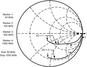
Table 8. OSCin Frequency
| FREQUENCY (MHz) | OSCin (NORMAL MODE) | OSCin (XO MODE) | OSCin# (NORMAL MODE) | |||
|---|---|---|---|---|---|---|
| REAL | IMAGINARY | REAL | IMAGINARY | REAL | IMAGINARY | |
| 1 | 3945.3 | 2261.6 | 9452.3 | 2182.1 | 3975.5 | 2287.0 |
| 5 | 4846.0 | –189.6 | 2397.9 | –916.7 | 4890.1 | –150.1 |
| 10 | 4253.4 | –1850.1 | 428.2 | –1105.7 | 4297.4 | –1886.7 |
| 20 | 2295.3 | –2366.9 | 248.4 | –591.8 | 2288.6 | –2383.8 |
| 30 | 1290.0 | –2087.0 | 187.1 | –410.1 | 1304.3 | –2079.1 |
| 40 | 847.9 | –1716.1 | 163.5 | –313.3 | 855.5 | –1718.0 |
| 50 | 581.3 | –1464.9 | 147.9 | –257.1 | 590.7 | –1471.6 |
| 60 | 439.2 | –1254.1 | 138.3 | –219.0 | 449.4 | –1264.2 |
| 70 | 337.9 | –1105.7 | 131.1 | –192.0 | 349.0 | –1115.4 |
| 80 | 269.4 | –983.6 | 127.0 | –171.8 | 276.3 | –989.1 |
| 90 | 223.4 | –869.9 | 119.7 | –158.0 | 231.9 | –876.2 |
| 100 | 179.2 | –776.8 | 114.5 | –143.9 | 186.9 | –783.9 |
| 200 | 52.4 | –379.8 | 93.9 | –85.1 | 54.3 | –382.5 |
| 300 | 31.2 | –247.0 | 80.9 | –68.9 | 31.9 | –247.4 |
| 400 | 23.5 | –181.7 | 72.3 | –58.1 | 23.8 | –180.5 |
| 500 | 20.4 | –140.5 | 65.1 | –49.4 | 20.4 | –138.4 |
| 600 | 18.4 | –110.2 | 58.1 | –42.1 | 18.2 | –107.6 |
| 700 | 17.0 | –88.0 | 51.9 | –35.6 | 16.7 | –85.3 |
| 800 | 15.8 | –71.2 | 47.4 | –29.5 | 15.7 | –68.4 |
| 900 | 15.2 | –57.6 | 43.6 | –23.4 | 14.7 | –56.3 |
| 1000 | 15.1 | –45.2 | 40.9 | –17.2 | 14.3 | –44.7 |
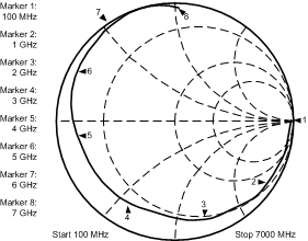
Table 9. ExtVCOin Frequency
| FREQUENCY | REAL | IMAGINARY |
|---|---|---|
| 100 | 627.9 | –1532.3 |
| 200 | 193.8 | –852.6 |
| 400 | 56.4 | –434.5 |
| 600 | 31.3 | –287.4 |
| 800 | 23.2 | –212.9 |
| 1000 | 17.8 | –167.0 |
| 1200 | 15.4 | –134.9 |
| 1400 | 14.0 | –111.4 |
| 1600 | 12.8 | –93.7 |
| 1800 | 11.8 | –79.5 |
| 2000 | 11.2 | –67.5 |
| 2200 | 10.7 | –57.4 |
| 2400 | 10.2 | –48.6 |
| 2600 | 10.5 | –42.0 |
| 2800 | 9.1 | –35.5 |
| 3000 | 7.8 | –29.0 |
| 3200 | 7.2 | –23.4 |
| 3400 | 6.6 | –18.3 |
| 3600 | 5.9 | –13.3 |
| 3800 | 5.3 | –8.5 |
| 4000 | 5.0 | –3.7 |
| 4200 | 4.5 | –1.4 |
| 4400 | 4.0 | 0.9 |
| 4600 | 3.5 | 3.1 |
| 4800 | 2.6 | 7.7 |
| 5000 | 1.7 | 12.1 |
| 6000 | 0.9 | 26.7 |
| 7000 | 2.3 | 51.9 |