JAJSFK8C June   2018  – November 2018 LMX2615-SP

PRODUCTION DATA.  

  1. 特長
  2. アプリケーション
  3. 概要
    1.     Device Images
      1.      概略回路図
  4. 改訂履歴
  5. Pin Configuration and Functions
    1.     Pin Functions
      1.      CQFP Package (QFN) Pin Functions
  6. Specifications
    1. 6.1 Absolute Maximum Ratings
    2. 6.2 ESD Ratings
    3. 6.3 Recommended Operating Conditions
    4. 6.4 Thermal Information
    5. 6.5 Electrical Characteristics
    6. 6.6 Timing Requirements
    7. 6.7 Typical Characteristics
  7. Detailed Description
    1. 7.1 Overview
    2. 7.2 Functional Block Diagram
    3. 7.3 Feature Description
      1. 7.3.1  Reference Oscillator Input
      2. 7.3.2  Reference Path
        1. 7.3.2.1 OSCin Doubler (OSC_2X)
        2. 7.3.2.2 Pre-R Divider (PLL_R_PRE)
        3. 7.3.2.3 Post-R Divider (PLL_R)
      3. 7.3.3  State Machine Clock
      4. 7.3.4  PLL Phase Detector and Charge Pump
      5. 7.3.5  N Divider and Fractional Circuitry
      6. 7.3.6  MUXout Pin
        1. 7.3.6.1 Serial data output for readback
        2. 7.3.6.2 Lock detect indicator set as type “VCOCal”
        3. 7.3.6.3 Lock detect indicator set as type “Vtune and VCOCal”
      7. 7.3.7  VCO (Voltage Controlled Oscillator)
        1. 7.3.7.1 VCO Calibration
        2. 7.3.7.2 Watchdog Feature
        3. 7.3.7.3 RECAL Feature
        4. 7.3.7.4 Determining the VCO Gain
      8. 7.3.8  Channel Divider
      9. 7.3.9  Output Buffer
      10. 7.3.10 Powerdown Modes
      11. 7.3.11 Treatment of Unused Pins
      12. 7.3.12 Phase Synchronization
        1. 7.3.12.1 General Concept
        2. 7.3.12.2 Categories of Applications for SYNC
        3. 7.3.12.3 Procedure for Using SYNC
        4. 7.3.12.4 SYNC Input Pin
      13. 7.3.13 Phase Adjust
      14. 7.3.14 Fine Adjustments for Phase Adjust and Phase SYNC
      15. 7.3.15 SYSREF
        1. 7.3.15.1 Programmable Fields
        2. 7.3.15.2 Input and Output Pin Formats
          1. 7.3.15.2.1 SYSREF Output Format
        3. 7.3.15.3 Examples
        4. 7.3.15.4 SYSREF Procedure
      16. 7.3.16 Pin Modes
    4. 7.4 Device Functional Modes
    5. 7.5 Programming
      1. 7.5.1 Recommended Initial Power-Up Sequence
      2. 7.5.2 Recommended Sequence for Changing Frequencies
    6. 7.6 Register Maps
      1. 7.6.1 Register Map
        1. 7.6.1.1  R0 Register (Address = 0x0) [reset = X]
          1. Table 22. R0 Register Field Descriptions
        2. 7.6.1.2  R1 Register (Address = 0x1) [reset = 0x4]
          1. Table 23. R1 Register Field Descriptions
        3. 7.6.1.3  R8 Register (Address = 0x8) [reset = X]
          1. Table 24. R8 Register Field Descriptions
        4. 7.6.1.4  R9 Register (Address = 0x9) [reset = X]
          1. Table 25. R9 Register Field Descriptions
        5. 7.6.1.5  R11 Register (Address = 0xB) [reset = 0x10]
          1. Table 26. R11 Register Field Descriptions
        6. 7.6.1.6  R12 Register (Address = 0xC) [reset = 0x1]
          1. Table 27. R12 Register Field Descriptions
        7. 7.6.1.7  R14 Register (Address = 0xE) [reset = 0x70]
          1. Table 28. R14 Register Field Descriptions
        8. 7.6.1.8  R16 Register (Address = 0x10) [reset = 0x80]
          1. Table 29. R16 Register Field Descriptions
        9. 7.6.1.9  R19 Register (Address = 0x13) [reset = 0xB7]
          1. Table 30. R19 Register Field Descriptions
        10. 7.6.1.10 R20 Register (Address = 0x14) [reset = X]
          1. Table 31. R20 Register Field Descriptions
        11. 7.6.1.11 R31 Register (Address = 0x1F) [reset = X]
          1. Table 32. R31 Register Field Descriptions
        12. 7.6.1.12 R34 Register (Address = 0x22) [reset = 0x0]
          1. Table 33. R34 Register Field Descriptions
        13. 7.6.1.13 R36 Register (Address = 0x24) [reset = 0x46]
          1. Table 34. R36 Register Field Descriptions
        14. 7.6.1.14 R37 Register (Address = 0x25) [reset = 0x400]
          1. Table 35. R37 Register Field Descriptions
        15. 7.6.1.15 R38 Register (Address = 0x26) [reset = 0xFD51]
          1. Table 36. R38 Register Field Descriptions
        16. 7.6.1.16 R39 Register (Address = 0x27) [reset = 0xDA80]
          1. Table 37. R39 Register Field Descriptions
        17. 7.6.1.17 R40 Register (Address = 0x28) [reset = 0x0]
          1. Table 38. R40 Register Field Descriptions
        18. 7.6.1.18 R41 Register (Address = 0x29) [reset = 0x0]
          1. Table 39. R41 Register Field Descriptions
        19. 7.6.1.19 R42 Register (Address = 0x2A) [reset = 0x0]
          1. Table 40. R42 Register Field Descriptions
        20. 7.6.1.20 R43 Register (Address = 0x2B) [reset = 0x0]
          1. Table 41. R43 Register Field Descriptions
        21. 7.6.1.21 R44 Register (Address = 0x2C) [reset = 0x1FA3]
          1. Table 42. R44 Register Field Descriptions
        22. 7.6.1.22 R45 Register (Address = 0x2D) [reset = X]
          1. Table 43. R45 Register Field Descriptions
        23. 7.6.1.23 R46 Register (Address = 0x2E) [reset = 0x1]
          1. Table 44. R46 Register Field Descriptions
        24. 7.6.1.24 R58 Register (Address = 0x3A) [reset = X]
          1. Table 45. R58 Register Field Descriptions
        25. 7.6.1.25 R59 Register (Address = 0x3B) [reset = 0x1]
          1. Table 46. R59 Register Field Descriptions
        26. 7.6.1.26 R60 Register (Address = 0x3C) [reset = 0x9C4]
          1. Table 47. R60 Register Field Descriptions
        27. 7.6.1.27 R69 Register (Address = 0x45) [reset = 0x0]
          1. Table 48. R69 Register Field Descriptions
        28. 7.6.1.28 R70 Register (Address = 0x46) [reset = 0xC350]
          1. Table 49. R70 Register Field Descriptions
        29. 7.6.1.29 R71 Register (Address = 0x47) [reset = 0x80]
          1. Table 50. R71 Register Field Descriptions
        30. 7.6.1.30 R72 Register (Address = 0x48) [reset = 0x1]
          1. Table 51. R72 Register Field Descriptions
        31. 7.6.1.31 R73 Register (Address = 0x49) [reset = 0x3F]
          1. Table 52. R73 Register Field Descriptions
        32. 7.6.1.32 R74 Register (Address = 0x4A) [reset = 0x0]
          1. Table 53. R74 Register Field Descriptions
        33. 7.6.1.33 R75 Register (Address = 0x4B) [reset = 0x0]
          1. Table 54. R75 Register Field Descriptions
        34. 7.6.1.34 R110 Register (Address = 0x6E) [reset = 0x0]
          1. Table 55. R110 Register Field Descriptions
        35. 7.6.1.35 R111 Register (Address = 0x6F) [reset = 0x0]
          1. Table 56. R111 Register Field Descriptions
        36. 7.6.1.36 R112 Register (Address = 0x70) [reset = 0x0]
          1. Table 57. R112 Register Field Descriptions
        37. 7.6.1.37 R113 Register (Address = 0x71) [reset = 0x0]
          1. Table 58. R113 Register Field Descriptions
        38. 7.6.1.38 R114 Register (Address = 0x72) [reset = 0x26F]
          1. Table 59. R114 Register Field Descriptions
  8. Application and Implementation
    1. 8.1 Application Information
      1. 8.1.1 OSCin Configuration
      2. 8.1.2 OSCin Slew Rate
      3. 8.1.3 RF Output Buffer Power Control
      4. 8.1.4 RF Output Buffer Pullup
        1. 8.1.4.1 Resistor Pullup
        2. 8.1.4.2 Inductor Pullup
        3. 8.1.4.3 Combination Pullup
      5. 8.1.5 RF Output Treatment for the Complimentary Side
        1. 8.1.5.1 Single-Ended Termination of Unused Output
        2. 8.1.5.2 Differential Termination
    2. 8.2 Typical Application
      1. 8.2.1 Design Requirements
      2. 8.2.2 Detailed Design Procedure
      3. 8.2.3 Application Curve
  9. Power Supply Recommendations
  10. 10Layout
    1. 10.1 Layout Guidelines
    2. 10.2 Layout Example
    3. 10.3 Footprint Example on PCB Layout
    4. 10.4 Radiation Environments
      1. 10.4.1 Total Ionizing Dose
      2. 10.4.2 Single Event Effect
  11. 11デバイスおよびドキュメントのサポート
    1. 11.1 デバイス・サポート
      1. 11.1.1 デベロッパー・ネットワークの製品に関する免責事項
      2. 11.1.2 開発サポート
    2. 11.2 ドキュメントのサポート
      1. 11.2.1 関連資料
    3. 11.3 商標
    4. 11.4 静電気放電に関する注意事項
    5. 11.5 Glossary
  12. 12メカニカル、パッケージ、および注文情報
    1. 12.1 エンジニアリング・サンプル
    2. 12.2 パッケージ・メカニカル情報

パッケージ・オプション

メカニカル・データ(パッケージ|ピン)
サーマルパッド・メカニカル・データ
発注情報

Typical Characteristics

LMX2615-SP tc_PN_8p1G.gif
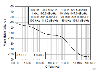
fOSC = 100 MHz Jitter = 53.0 fs (100 Hz - 100 MHz)
fPD = 200 MHz
Figure 3. Closed Loop Phase Noise at 8.1 GHz
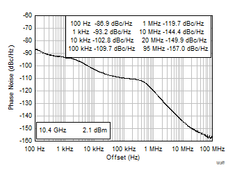
LMX2615-SP tc_PN_10p4G.gif
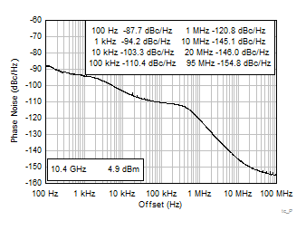
fOSC = 100 MHz Jitter = 57.6 fs (100 Hz - 100 MHz)
fPD = 200 MHz
Figure 5. Closed Loop Phase Noise at 10.4 GHz
LMX2615-SP tc_PN_12p5G.gif
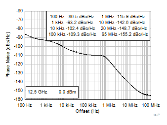
fOSC = 100 MHz Jitter = 62.4 fs (100 Hz - 100 MHz)
fPD = 200 MHz
Figure 7. Closed Loop Phase Noise at 12.5 GHz
LMX2615-SP tc_PN_14p7G.gif
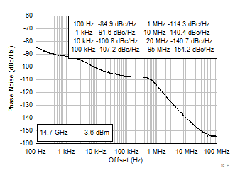
fOSC = 100 MHz Jitter = 65.5 fs (100 Hz - 100 MHz)
fPD = 200 MHz
Figure 9. Closed Loop Phase Noise at 14.7 GHz

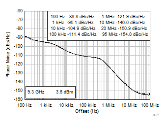
LMX2615-SP tc_PN_9p3G.gif
fOSC = 100 MHz Jitter = 56.7 fs (100 Hz - 100 MHz)
fPD = 200 MHz
Figure 4. Closed Loop Phase Noise at 9.3 GHz
LMX2615-SP tc_PN_11p4G.gif
fOSC = 100 MHz Jitter = 57.8 fs (100 Hz - 100 MHz)
fPD = 200 MHz
Figure 6. Closed Loop Phase Noise at 11.4 GHz
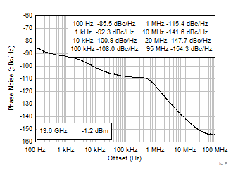
LMX2615-SP tc_PN_13p6G.gif
fOSC = 100 MHz fOUT = 14 GHz/2 = 3.5 GHz
fPD = 200 MHz Jitter = 64.2 fs (100 Hz - 100 MHz)
fVCO = 14 GHz
Figure 8. Closed Loop Phase Noise at 13.6 GHz
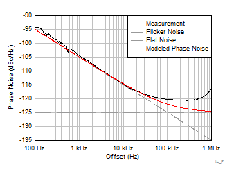
LMX2615-SP tc_PN_Metrics.gif
fVCO = 10 GHz fPD = 200 MHz
FOM = -237.5 Flicker = -130.5
Figure 10. Calculation of PLL Noise Metrics
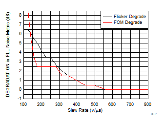
LMX2615-SP tc_PN_Metrics_SlewRate.gif
fOSC = 200 MHz fVCO = 14.8 GHz
Figure 11. PLL Phase Noise Metrics vs. Fosc Slew Rate
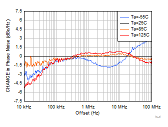
LMX2615-SP tc_dPN_VCO_TEMP.gif
fVCO = 10 GHz, Narrow Loop Bandwidth (<100 Hz) VCO Re-Calibrated at Final Frequency
Figure 12. CHANGE in VCO Phase Noise Over Temperature
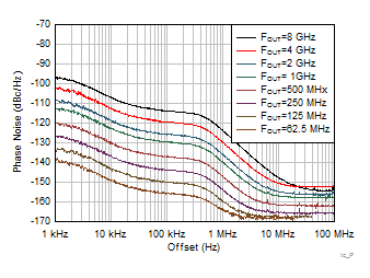
LMX2615-SP tc_PN_VCODIV.gif
Figure 14. Divided Output Frequency
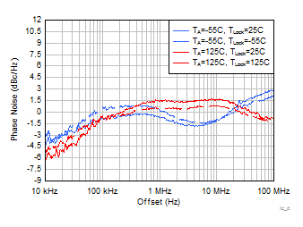
LMX2615-SP tc_dPN_VCO_dTEMP.gif
fVCO = 10 GHz, Narrow Loop Bandwidth (<100 Hz) VCO Calibrated at 25C and Temperature Drifted
Figure 13. CHANGE in 8 GHz VCO Phase Noise Over Temperature
LMX2615-SP tc_PN_VCODIV_Analysis.gif
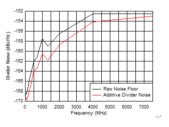
This noise adds to the scaled VCO Noise when the channel divider is used.
Figure 15. Additive VCO Divider Noise Floor
LMX2615-SP tc_PWR_PullUp.gif
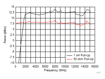
Single-Ended Output OUTx_PWR = 31
Figure 16. Output Power vs Pull-up
LMX2615-SP tc_PWR_OUTx_PWR.gif
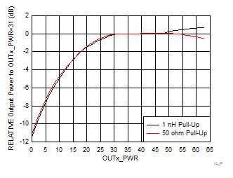
Single-Ended Output OUTx_PWR=31
Figure 18. Impact of OUTx_PWR on Output Power
LMX2615-SP tc_PWR_TEMP.gif
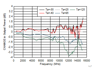
Single-ended output OUTx_PWR=31
Figure 17. CHANGE in Output Power vs Temperature
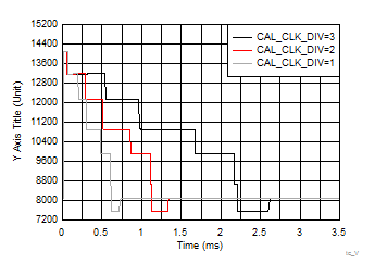
LMX2615-SP tc_VCOCAL_CAL_CLK_DIV.gif
fOSC = 100 MHz VCO_SEL = VCO7
fPD = 200 MHz FCAL_HPFD_ADJ=3
Figure 19. Impact of CAL_CLK_DIV on VCO Calibration Time
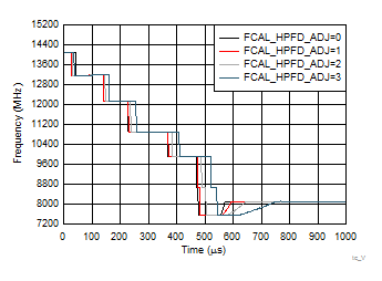
LMX2615-SP tc_VCOCAL_HPFD_ADJ.gif
fOSC = 100 MHz VCO_SEL=VCO7
fPD = 500 MHz CAL_CLK_DIV=2
Figure 21. Impact of FCAL_HPFD_ADJ on VCO Calibration Time
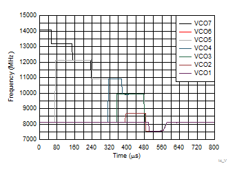
LMX2615-SP tc_VCOCAL_VCO_SEL.gif
fOSC = 100 MHz FCAL_HPFD_ADJ=2
fPD = 200 MHz CAL_CLK_DIV=2
Figure 20. Impact of VCO_SEL on VCO Calibration Time