SNVS322M December 2004 – December 2015 LP38690 , LP38692
PRODUCTION DATA.
- 1 Features
- 2 Applications
- 3 Description
- 4 Revision History
- 5 Pin Configuration and Functions
- 6 Specifications
- 7 Detailed Description
- 8 Application and Implementation
- 9 Power Supply Recommendations
- 10Layout
- 11Device and Documentation Support
- 12Mechanical, Packaging, and Orderable Information
1 Features
- Wide Input Voltage Range (2.7 V to 10 V)
- 2.5% Output Accuracy (25°C)
- Low Dropout Voltage: 450 mV at 1 A
(typical, 5 VOUT) - Precision (Trimmed) Bandgap Reference
- Ensured Specifications for –40°C to 125°C
- 1-µA Off-State Quiescent Current
- Thermal Overload Protection
- Foldback Current Limiting
- 3-Lead TO-252, 5-Lead SOT-223, and 6-Bump WSON Packages
- Enable Pin (LP38692)
- Ground Pin Current: 55 µA (typical) at Full Load
- Precision Output Voltage: 2.5% (25°C) Accuracy
2 Applications
- Hard Disk Drives
- Notebook Computers
- Battery Powered Devices
- Portable Instrumentation
3 Description
The LP38690 and LP38692 low-dropout CMOS linear regulators provide tight output tolerance (2.5% typical), extremely low dropout voltage (450 mV at a 1-A load current, VOUT = 5 V), and excellent AC performance utilizing ultra low ESR ceramic output capacitors.
The low thermal resistance of the WSON, SOT-223, and TO-252 packages allow the full operating current to be used even in high ambient temperature environments.
The use of a PMOS power transistor means that no DC base drive current is required to bias it allowing ground pin current to remain below 100 µA regardless of load current, input voltage, or operating temperature.
Device Information(1)
| PART NUMBER | PACKAGE | BODY SIZE (NOM) |
|---|---|---|
| LP38690 | TO-252 (3) | 6.58 mm x 6.10 mm |
| WSON (6) | 3.00 mm x 3.00 mm | |
| LP38692 | SOT-223 (5) | 6.50 mm x 3.56 mm |
| WSON (6) | 3.00 mm x 3.00 mm |
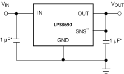
Simplified Schematic for LP38690

* Minimum value required for stability.
**WSON package devices only.
**WSON package devices only.
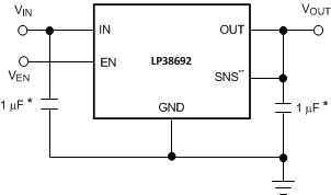
Simplified Schematic for LP38692

* Minimum value required for stability.
**WSON package devices only.
**WSON package devices only.