SNVS311D May 2005 – February 2015 LP3878-ADJ
PRODUCTION DATA.
- 1 Features
- 2 Applications
- 3 Description
- 4 Revision History
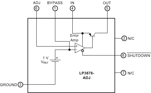
- 5 Pin Configuration and Functions
- 6 Specifications
- 7 Detailed Description
- 8 Application and Implementation
- 9 Power Supply Recommendations
- 10Layout
- 11Device and Documentation Support
- 12Mechanical, Packaging, and Orderable Information
パッケージ・オプション
メカニカル・データ(パッケージ|ピン)
サーマルパッド・メカニカル・データ
- DDA|8
発注情報
7 Detailed Description
7.1 Overview
The LP3878-ADJ is an adjustable regulator; the output voltage can be set from 1 V to 5.5 V. The device can deliver 800-mA continuous load current. Standard regulator features, such as overcurrent and overtemperature protection, are also included.
The LP3878-ADJ contains other features:
- Low power shutdown current and low ground pin current
- Very low output noise
- 8-lead SO PowerPAD or WSON surface-mount packages to allow for increased power dissipation.
7.2 Functional Block Diagram
7.3 Feature Description
7.3.1 Shutdown Input Operation
The LP3878-ADJ is shut off by pulling the SHUTDOWN input low, and turned on by pulling it high. If this feature is not to be used, the SHUTDOWN input should be tied to VIN to keep the regulator output on at all times.
To assure proper operation, the signal source used to drive the SHUTDOWN input must be able to swing above and below the specified turnon or turnoff voltage thresholds listed in the Electrical Characteristics under VON/OFF.
7.3.2 Reverse Input-Output Voltage
The PNP power transistor used as the pass element in the LP3878-ADJ contains a parasitic diode between the IN pin and the OUT pin. During normal operation (where the IN pin voltage is higher than the OUT pin voltage) this parasitic diode is reverse-biased. However, if the OUT pin voltage is pulled above the IN pin voltage this diode will turn ON, and current will flow into the LP3878-ADJ OUT pin.
In such cases, a parasitic SCR between the IN pin and the GND pin can latch ON which will allow a high current to flow from the VIN supply, into the IN pin to ground, which can damage the part. In any application where the OUT pin voltage may be higher than the IN pin voltage, even momentarily, an external Schottky diode must be connected from the IN pin to the OUT pin (cathode to IN pin, anode to OUT pin), to limit the reverse voltage across the LP3878-ADJ to 0.3 V (see Absolute Maximum Ratings).
7.3.3 Low Output Noise
With a 10-nF capacitor on the BYPASS pin, the output noise is only 18 µV.
7.4 Device Functional Modes
7.4.1 Operation With VOUT(TARGET) + 2 V ≤ VIN ≤ 16 V
The device operates if the input voltage is equal to, or exceeds VOUT(TARGET) + 2 V. At input voltages below the minimum VIN requirement, the device does not operate correctly and output voltage may not reach target value.
7.4.2 Operation With SHUTDOWN Pin Control
LP3878-ADJ is turned off by pulling the SHUTDOWN pin low, and turned on by pulling it high. If this feature is not used, the SHUTDOWN pin should be tied to VIN to keep the regulator output on at all times. To assure proper operation, the signal source used to drive the SHUTDOWN input must be able to swing above and below the specified turnon and turnoff voltage thresholds listed in the Electrical Characteristics under VL and VH.