JAJSE29A August   2017  – December 2017 LPV821

PRODUCTION DATA.  

  1. 特長
  2. アプリケーション
  3. 概要
    1.     Device Images
      1.      ローサイド、常時オンの電流検出
  4. 改訂履歴
  5. 概要(続き)
  6. Pin Configuration and Functions
    1.     Pin Functions: LPV821 DBV
    2.     Pin Functions: LPV822 DSG (Preview)
  7. Specifications
    1. 7.1 Absolute Maximum Ratings
    2. 7.2 ESD Ratings
    3. 7.3 Recommended Operating Conditions
    4. 7.4 Thermal Information
    5. 7.5 Electrical Characteristics
    6. 7.6 Typical Characteristics
  8. Detailed Description
    1. 8.1 Overview
    2. 8.2 Functional Block Diagram
    3. 8.3 Feature Description
      1. 8.3.1 Operating Voltage
      2. 8.3.2 Input
      3. 8.3.3 Internal Offset Correction
      4. 8.3.4 Input Offset Voltage Drift
    4. 8.4 Device Functional Modes
      1. 8.4.1 EMI Performance and Input Filtering
      2. 8.4.2 Driving Capacitive Load
  9. Application and Implementation
    1. 9.1 Application Information
    2. 9.2 Typical Applications
      1. 9.2.1 Low-Side Current Measurement
        1. 9.2.1.1 Design Requirements
        2. 9.2.1.2 Detailed Design Procedure
  10. 10Power Supply Recommendations
  11. 11Layout
    1. 11.1 Layout Guidelines
      1. 11.1.1 General Layout Guidelines
    2. 11.2 Layout Example
  12. 12デバイスおよびドキュメントのサポート
    1. 12.1 デバイス・サポート
      1. 12.1.1 開発サポート
    2. 12.2 関連リンク
    3. 12.3 ドキュメントの更新通知を受け取る方法
    4. 12.4 コミュニティ・リソース
    5. 12.5 商標
    6. 12.6 静電気放電に関する注意事項
    7. 12.7 Glossary
  13. 13メカニカル、パッケージ、および注文情報

パッケージ・オプション

メカニカル・データ(パッケージ|ピン)
サーマルパッド・メカニカル・データ
発注情報

Typical Characteristics

At TA = 25°C, VS = 3.3 V, VCM = VOUT = VS/2, CL = 20 pF, and RL≥ 10 MΩ, unless otherwise noted.
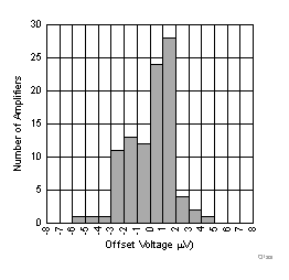
LPV821 OfssetVoltage1_8m40_fixed.gif
VS = 1.8 V N = 98 units TA = -40°C
Figure 1. Offset Voltage Distribution, Vs = 1.8 V
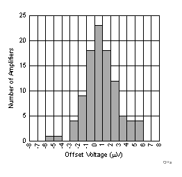
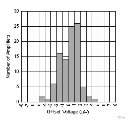
LPV821 OffsetVoltage_1_8_125_fixed.gif
VS = 1.8 V N = 98 units TA = 125°C
Figure 3. Offset Voltage Distribution, Vs = 1.8 V
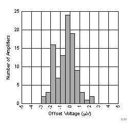
LPV821 3.3VOffsetHistogramSmaller.gif
VS = 3.3 V N = 98 units TA = 25°C
Figure 5. Offset Voltage Distribution, Vs = 3.3 V
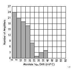
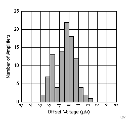
LPV821 1.8V_99_Units_HistogramSmaller.gif
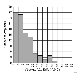
VS = 1.8 V N = 98 units
Figure 7. Offset Voltage Drift Distribution, Vs = 1.8 V
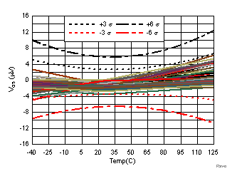
LPV821 Rawoffset99unitsremovedlabels.gif
VS = 3.3 V N = 98 units
Figure 9. Offset Voltage vs Temperature, Vs = 3.3 V
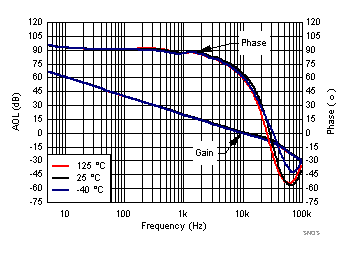
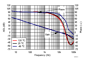
LPV821 SNOSD36_Gain_Phase_1p8_3T.gif
VS = 1.8 V CL = 20 pF TA = –40, 25, 125°C
Figure 11. Open-Loop Gain and Phase vs Frequency
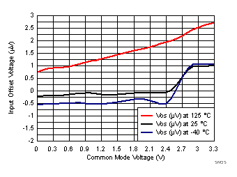
LPV821 SNOSD36_VOS_Vcm_3T-1p8V.gif
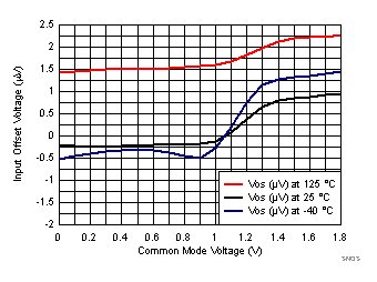
VS = 1.8 V
Figure 13. Input Offset Voltage vs Input Common Mode Voltage
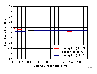
LPV821 SNOSD36_Ib_INP_vs_Vcm_3T_VS_1p8V.gif
VS = 1.8 V
Figure 15. Input Bias Current on +IN Input Pin vs Common Mode Voltage
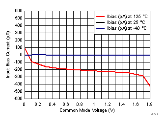
LPV821 SNOSD36_Ib_INM_vs_Vcm_3T_VS_1p8V.gif
VS = 1.8 V
Figure 17. Input Bias Current on –IN Pin vs Common Mode Voltage
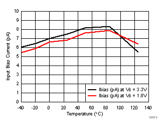
LPV821 SNOSD36_Ibias_INP_vs_Temp.gif
VS = 3.3 V and 1.8 V
Figure 19. Input Bias Current ON +IN Input vs Temperature
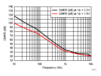
LPV821 SNOSD36_CMRR_vs_Freq.gif
VS = 3.3 V and 1.8 V
Figure 21. CMRR vs Frequency
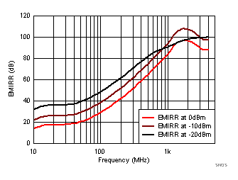
LPV821 SNOSD36_EMIRR_vs_Fr-3p3V.gif
Figure 23. EMIRR Performance
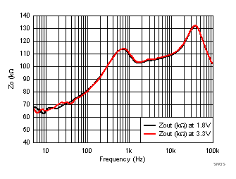
LPV821 SNOSD36_Z_out_vs_F-3p3V_1.8V.gif
VS = 3.3 V and 1.8 V
Figure 25. Open Loop Output Impedance
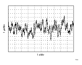
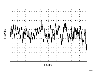
LPV821 NoisevsTime_3_3factor_thinner.gif
VS = 3.3 V
Figure 27. 0.1-Hz to 10-Hz Noise, Vs = 3.3 V
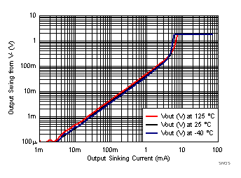
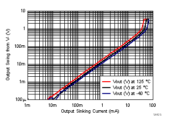
LPV821 SNOSD36_VOL_vs_Iout_sink_1p8V.gif
VS = 1.8 V TA = –40, 25, 125°C
Figure 29. Output Swing vs. Sinking Current, 1.8 V
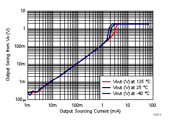
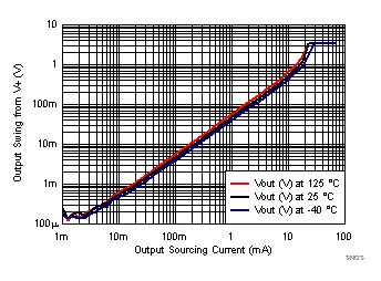
LPV821 SNOSD36_VOH_vs_Iout_Sours_1p8V.gif
VS = 1.8 V TA = –40, 25, 125°C
Figure 31. Output Swing vs Sourcing Current, 1.8 V
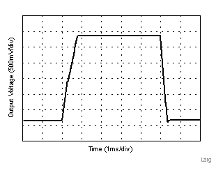
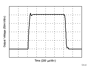
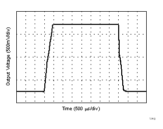
LPV821 LargeSignal3_3_without_label.gif
VIN = 2.64 VPP G = 1 RL = 1 MΩ
Figure 33. Large-Signal Response, 3.3V
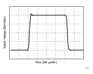
LPV821 SmallSignal3_3_fixed.gif
VIN = 0.2 VPP G = 1 RL = 1 MΩ
Figure 35. Small Signal Response, 3.3V
LPV821 1.8VOffsetHistogramSmaller.gif
VS = 1.8 V N = 98 units TA = 25°C
Figure 2. Offset Voltage Distribution, Vs = 1.8 V
LPV821 OffsetVoltage_3_3m40_fixed.gif
VS = 3.3 V N = 98 units TA = -40°C
Figure 4. Offset Voltage Distribution, Vs = 3.3 V
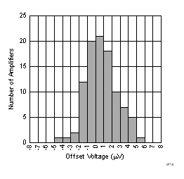
LPV821 offsetVoltage3_3125.gif
VS = 3.3 V N = 98 units TA = 125°C
Figure 6. Offset Voltage Distribution, Vs = 3.3 V
LPV821 3.3V99UnitsHistogramSmaller.gif
VS = 3.3 V N = 98 units
Figure 8. Offset Voltage Drift Distribution, Vs = 3.3 V
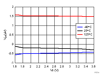
LPV821 VOSvsVSwith3temprangesplottedfixed2.gif
TA = –40, 25, 125°C
Figure 10. Offset Voltage vs Supply Voltage
LPV821 SNOSD36_Gain_Phase_3p3_3T.gif
VS = 3.3 V CL = 20 pF TA = –40, 25, 125°C
Figure 12. Open-Loop Gain and Phase vs Frequency
LPV821 SNOSD36_VOS_Vcm_3T-3p3V.gif
VS = 3.3 V
Figure 14. Input Offset Voltage vs Input Common Mode Voltage
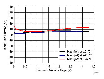
LPV821 SNOSD36_Ib_INP_vs_Vcm_3T_VS_3p3V.gif
VS = 3.3 V
Figure 16. Input Bias Current on +IN Input Pin vs Common Mode Voltage
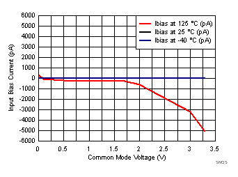
LPV821 SNOSD36_Ib_INM_vs_Vcm_3T_VS_3p3V.gif
VS = 3.3 V
Figure 18. Input Bias Current on –IN Input Pin vs Common Mode Voltage
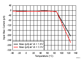
LPV821 SNOSD36_Ibias_INM_vs_Temp.gif
VS = 3.3 V and 1.8 V
Figure 20. Input Bias Current on –IN Input Pin vs Temperature
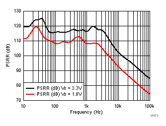
LPV821 SNOSD36_PSRR_vs_Freq.gif
VS = 3.3 V and 1.8 V
Figure 22. PSRR vs Frequency
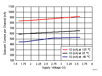
LPV821 SNOSD36_IQ-vs_Vs_3T.gif
TA = –40, 25, 125°C
Figure 24. Per Channel Quiescent Current vs Supply Voltage
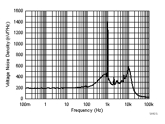
LPV821 SNOSD36_Noise_vs_Fre.gif
Figure 26. Voltage Noise Spectral Density vs Frequency
LPV821 NoisevsTime_1_8factor_thinner.gif
VS = 1.8 V
Figure 28. 0.1-Hz to 10-Hz Noise, Vs = 1.8 V
LPV821 SNOSD36_VOL_vs_Iout_sink_3p3V.gif
VS = 3.3 V TA = –40, 25, 125°C
Figure 30. Output Swing vs. Sinking Current, 3.3 V
LPV821 SNOSD36_VOH_vs_Iout_Sours_3p3V.gif
VS = 3.3 V TA = –40, 25, 125°C
Figure 32. Output Swing vs Sourcing Current, 3.3 V
LPV821 LargeSignal1_8.gif
VIN = 1.44 VPP G = 1 RL = 1 MΩ
Figure 34. Large-Signal Response, 1.8V
LPV821 SmallSignal1_8_without_label_fixed.gif
VIN = 0.2 VPP G = 1 RL = 1 MΩ
Figure 36. Small-Signal Response, 1.8V