JAJSFL3B November 2010 – June 2018 MSP430AFE221 , MSP430AFE222 , MSP430AFE223 , MSP430AFE231 , MSP430AFE232 , MSP430AFE233 , MSP430AFE251 , MSP430AFE252 , MSP430AFE253
PRODUCTION DATA.
- 1デバイスの概要
- 2改訂履歴
- 3Device Comparison
- 4Terminal Configuration and Functions
-
5Specifications
- 5.1 Absolute Maximum Ratings
- 5.2 ESD Ratings
- 5.3 Recommended Operating Conditions
- 5.4 Thermal Resistance Characteristics for PW-24 Package
- 5.5 Active Mode Supply Current (Into DVCC and AVCC) Excluding External Current
- 5.6 Typical Characteristics – Active-Mode Supply Current (Into DVCC and AVCC)
- 5.7 Low-Power-Mode Supply Currents (Into VCC) Excluding External Current
- 5.8 Typical Characteristics – LPM4 Current
- 5.9 Schmitt-Trigger Inputs (Ports Px and RST/NMI)
- 5.10 Leakage Current (Ports Px)
- 5.11 Outputs (Ports Px)
- 5.12 Output Frequency (Ports Px)
- 5.13 Typical Characteristics – Outputs
- 5.14 POR, BOR
- 5.15 Typical Characteristics – POR, BOR
- 5.16 Supply Voltage Supervisor (SVS), Supply Voltage Monitor (SVM)
- 5.17 Main DCO Characteristics
- 5.18 DCO Frequency
- 5.19 Calibrated DCO Frequencies – Tolerance
- 5.20 Wake-up Times From Lower-Power Modes (LPM3, LPM4)
- 5.21 Typical Characteristics – DCO Clock Wake-up Time
- 5.22 Internal Very-Low-Power Low-Frequency Oscillator (VLO)
- 5.23 Crystal Oscillator (XT2)
- 5.24 Typical Characteristics – XT2 Oscillator
- 5.25 SD24_A, Power Supply
- 5.26 SD24_A, Input Range
- 5.27 SD24_A, Performance
- 5.28 SD24_A, Temperature Sensor and Built-In VCC Sense
- 5.29 SD24_A, Built-In Voltage Reference
- 5.30 SD24_A, Reference Output Buffer
- 5.31 SD24_A, External Reference Input
- 5.32 USART0
- 5.33 Timer_A3
- 5.34 Flash Memory
- 5.35 RAM
- 5.36 JTAG and Spy-Bi-Wire Interface
- 5.37 JTAG Fuse
-
6Detailed Description
- 6.1 CPU
- 6.2 Instruction Set
- 6.3 Operating Modes
- 6.4 Interrupt Vector Addresses
- 6.5 Special Function Registers
- 6.6 Memory Organization
- 6.7 Flash Memory
- 6.8 Peripherals
- 6.9 Oscillator and System Clock
- 6.10 Brownout, Supply Voltage Supervisor
- 6.11 Digital I/O
- 6.12 Watchdog Timer (WDT+)
- 6.13 Timer_A3
- 6.14 USART0
- 6.15 Hardware Multiplier
- 6.16 SD24_A
- 6.17 Peripheral File Map
- 6.18
I/O Port Schematics
- 6.18.1 Port P1 Pin Schematic: P1.0 Input/Output With Schmitt Trigger
- 6.18.2 Port P1 Pin Schematic: P1.1 and P1.2 Input/Output With Schmitt Trigger
- 6.18.3 Port P1 Pin Schematic: P1.3 Input/Output With Schmitt Trigger
- 6.18.4 Port P1 Pin Schematic: P1.4 Input/Output With Schmitt Trigger
- 6.18.5 Port P1 Pin Schematic: P1.5 to P1.7 Input/Output With Schmitt Trigger
- 6.18.6 Port P2 Pin Schematic: P2.0 Input/Output With Schmitt Trigger
- 6.18.7 Port P2 Pin Schematic: P2.6, Input/Output With Schmitt Trigger
- 6.18.8 Port P2 Pin Schematic: P2.7, Input/Output With Schmitt Trigger
- 6.18.9 JTAG Fuse Check Mode
- 7デバイスおよびドキュメントのサポート
- 8メカニカル、パッケージ、および注文情報
7.2 Device Nomenclature
To designate the stages in the product development cycle, TI assigns prefixes to the part numbers of all MSP430 MCU devices and support tools. Each MSP430 MCU commercial family member has one of three prefixes: MSP, PMS, or XMS (for example, MSP430F5438A). TI recommends two of three possible prefix designators for its support tools: MSP and MSPX. These prefixes represent evolutionary stages of product development from engineering prototypes (with XMS for devices and MSPX for tools) through fully qualified production devices and tools (with MSP for devices and MSP for tools).
Device development evolutionary flow:
XMS – Experimental device that is not necessarily representative of the electrical specifications for the final device
PMS – Final silicon die that conforms to the electrical specifications for the device but has not completed quality and reliability verification
MSP – Fully qualified production device
Support tool development evolutionary flow:
MSPX – Development-support product that has not yet completed TI's internal qualification testing.
MSP – Fully-qualified development-support product
XMS and PMS devices and MSPX development-support tools are shipped against the following disclaimer:
"Developmental product is intended for internal evaluation purposes."
MSP devices and MSP development-support tools have been characterized fully, and the quality and reliability of the device have been demonstrated fully. TI's standard warranty applies.
Predictions show that prototype devices (XMS and PMS) have a greater failure rate than the standard production devices. TI recommends that these devices not be used in any production system because their expected end-use failure rate still is undefined. Only qualified production devices are to be used.
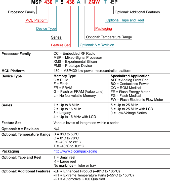
TI device nomenclature also includes a suffix with the device family name. This suffix indicates the package type (for example, PZP) and temperature range (for example, T). Figure 7-1 provides a legend for reading the complete device name for any family member.
 Figure 7-1 Device Nomenclature