SLAS508K April 2006 – May 2020 MSP430FG4616 , MSP430FG4617 , MSP430FG4618 , MSP430FG4619
PRODUCTION DATA.
- 1Device Overview
- 2Revision History
- 3Device Comparison
- 4Terminal Configuration and Functions
-
5Specifications
- 5.1 Absolute Maximum Ratings
- 5.2 ESD Ratings
- 5.3 Recommended Operating Conditions
- 5.4 Supply Current Into AVCC + DVCC Excluding External Current
- 5.5 Thermal Characteristics
- 5.6 Schmitt-Trigger Inputs – Ports P1 to P10, RST/NMI, JTAG (TCK, TMS, TDI/TCLK,TDO/TDI)
- 5.7 Inputs Px.x, TAx, TBX
- 5.8 Leakage Current – Ports P1 to P10
- 5.9 Outputs – Ports P1 to P10
- 5.10 Output Frequency
- 5.11 Typical Characteristics – Outputs
- 5.12 Wake-up Timing From LPM3
- 5.13 RAM
- 5.14 LCD_A
- 5.15 Comparator_A
- 5.16 Typical Characteristics – Comparator_A
- 5.17 POR, BOR
- 5.18 SVS (Supply Voltage Supervisor and Monitor)
- 5.19 DCO
- 5.20 Crystal Oscillator, LFXT1 Oscillator
- 5.21 Crystal Oscillator, XT2 Oscillator
- 5.22 USCI (UART Mode)
- 5.23 USCI (SPI Master Mode)
- 5.24 USCI (SPI Slave Mode)
- 5.25 USCI (I2C Mode)
- 5.26 USART1
- 5.27 12-Bit ADC, Power Supply and Input Range Conditions
- 5.28 12-Bit ADC, External Reference
- 5.29 12-Bit ADC, Built-In Reference
- 5.30 12-Bit ADC, Timing Parameters
- 5.31 12-Bit ADC, Linearity Parameters
- 5.32 12-Bit ADC, Temperature Sensor and Built-In VMID
- 5.33 12-Bit DAC, Supply Specifications
- 5.34 12-Bit DAC, Linearity Specifications
- 5.35 12-Bit DAC, Output Specifications
- 5.36 12-Bit DAC, Reference Input Specifications
- 5.37 12-Bit DAC, Dynamic Specifications
- 5.38 12-Bit DAC, Dynamic Specifications Continued
- 5.39 Operational Amplifier OA, Supply Specifications
- 5.40 Operational Amplifier OA, Input/Output Specifications
- 5.41 Operational Amplifier OA, Dynamic Specifications
- 5.42 Operational Amplifier OA, Typical Characteristics
- 5.43 Operational Amplifier OA Feedback Network, Noninverting Amplifier Mode (OAFCx = 4)
- 5.44 Operational Amplifier OA Feedback Network, Inverting Amplifier Mode (OAFCx = 6)
- 5.45 Flash Memory (FG461x Devices Only)
- 5.46 JTAG Interface
- 5.47 JTAG Fuse
-
6Detailed Description
- 6.1 CPU
- 6.2 Instruction Set
- 6.3 Operating Modes
- 6.4 Interrupt Vector Addresses
- 6.5 Special Function Registers (SFRs)
- 6.6 Memory Organization
- 6.7 Bootstrap Loader (BSL)
- 6.8 Flash Memory
- 6.9
Peripherals
- 6.9.1 DMA Controller
- 6.9.2 Oscillator and System Clock
- 6.9.3 Brownout, Supply Voltage Supervisor (SVS)
- 6.9.4 Digital I/O
- 6.9.5 Basic Timer1 and Real-Time Clock
- 6.9.6 LCD_A Drive With Regulated Charge Pump
- 6.9.7 Watchdog Timer (WDT+)
- 6.9.8 Universal Serial Communication Interface (USCI)
- 6.9.9 USART1
- 6.9.10 Hardware Multiplier
- 6.9.11 Timer_A3
- 6.9.12 Timer_B7
- 6.9.13 Comparator_A
- 6.9.14 ADC12
- 6.9.15 DAC12
- 6.9.16 OA
- 6.9.17 Peripheral File Map
- 6.10
Input/Output Schematics
- 6.10.1 Port P1, P1.0 to P1.5, Input/Output With Schmitt Trigger
- 6.10.2 Port P1, P1.6, P1.7, Input/Output With Schmitt Trigger
- 6.10.3 Port P2, P2.0 to P2.3, P2.6 to P2.7, Input/Output With Schmitt Trigger
- 6.10.4 Port P2, P2.4 to P2.5, Input/Output With Schmitt Trigger
- 6.10.5 Port P3, P3.0 to P3.3, Input/Output With Schmitt Trigger
- 6.10.6 Port P3, P3.4 to P3.7, Input/Output With Schmitt Trigger
- 6.10.7 Port P4, P4.0 to P4.1, Input/Output With Schmitt Trigger
- 6.10.8 Port P4, P4.2 to P4.7, Input/Output With Schmitt Trigger
- 6.10.9 Port P5, P5.0, Input/Output With Schmitt Trigger
- 6.10.10 Port P5, P5.1, Input/Output With Schmitt Trigger
- 6.10.11 Port P5, P5.2 to P5.4, Input/Output With Schmitt Trigger
- 6.10.12 Port P5, P5.5 to P5.7, Input/Output With Schmitt Trigger
- 6.10.13 Port P6, P6.0, P6.2, and P6.4, Input/Output With Schmitt Trigger
- 6.10.14 Port P6, P6.1, P6.3, and P6.5 Input/Output With Schmitt Trigger
- 6.10.15 Port P6, P6.6, Input/Output With Schmitt Trigger
- 6.10.16 Port P6, P6.7, Input/Output With Schmitt Trigger
- 6.10.17 Port P7, P7.0 to P7.3, Input/Output With Schmitt Trigger
- 6.10.18 Port P7, P7.4 to P7.7, Input/Output With Schmitt Trigger
- 6.10.19 Port P8, P8.0 to P8.7, Input/Output With Schmitt Trigger
- 6.10.20 Port P9, P9.0 to P9.7, Input/Output With Schmitt Trigger
- 6.10.21 Port P10, P10.0 to P10.5, Input/Output With Schmitt Trigger
- 6.10.22 Port P10, P10.6, Input/Output With Schmitt Trigger
- 6.10.23 Port P10, P10.7, Input/Output With Schmitt Trigger
- 6.10.24 VeREF+/DAC0
- 6.10.25 JTAG Pins TMS, TCK, TDI/TCLK, TDO/TDI, Input/Output With Schmitt Trigger or Output
- 6.10.26 JTAG Fuse Check Mode
-
7Device and Documentation Support
- 7.1 Device Support
- 7.2 Documentation Support
- 7.3 Related Links
- 7.4 Community Resources
- 7.5 Trademarks
- 7.6 Electrostatic Discharge Caution
- 7.7 Export Control Notice
- 7.8 Glossary
- 8Mechanical, Packaging, and Orderable Information
パッケージ・オプション
メカニカル・データ(パッケージ|ピン)
サーマルパッド・メカニカル・データ
- PZ|100
発注情報
5.34 12-Bit DAC, Linearity Specifications
over recommended ranges of supply voltage and operating free-air temperature (unless otherwise noted) (see Figure 5-26)| PARAMETER | TEST CONDITIONS | VCC | MIN | TYP | MAX | UNIT | |
|---|---|---|---|---|---|---|---|
| Resolution | 12-bit monotonic | 12 | bits | ||||
| INL | Integral nonlinearity(1) | Vref = 1.5 V,
DAC12AMPx = 7, DAC12IR = 1 |
2.2 V | ±2.0 | ±8.0 | LSB | |
| Vref = 2.5 V,
DAC12AMPx = 7, DAC12IR = 1 |
3 V | ||||||
| DNL | Differential nonlinearity(1) | Vref = 1.5 V,
DAC12AMPx = 7, DAC12IR = 1 |
2.2 V | ±0.4 | ±1.0 | LSB | |
| Vref = 2.5 V,
DAC12AMPx = 7, DAC12IR = 1 |
3 V | ||||||
| EO | Offset voltage without calibration(1)(2) | Vref = 1.5 V,
DAC12AMPx = 7, DAC12IR = 1 |
2.2 V | ±21 | mV | ||
| Vref = 2.5 V,
DAC12AMPx = 7, DAC12IR = 1 |
3 V | ||||||
| Offset voltage with calibration(1)(2) | Vref = 1.5 V,
DAC12AMPx = 7, DAC12IR = 1 |
2.2 V | ±2.5 | ||||
| Vref = 2.5 V,
DAC12AMPx = 7, DAC12IR = 1 |
3 V | ||||||
| dE(O)/dT | Offset error temperature coefficient(1) | 2.2 V, 3 V | ±30 | µV/°C | |||
| EG | Gain error(1) | VREF = 1.5 V | 2.2 V | ±3.5 | %FSR | ||
| VREF = 2.5 V | 3 V | ||||||
| dE(G)/dT | Gain temperature coefficient(1) | 2.2 V, 3 V | 10 | ppm of FSR/°C | |||
| tOffset_Cal | Time for offset calibration(3) | DAC12AMPx = 2 | 2.2 V, 3 V | 100 | ms | ||
| DAC12AMPx = 3, 5 | 32 | ||||||
| DAC12AMPx = 4, 6, 7 | 6 | ||||||
(1) Parameters calculated from the best-fit curve from 0x0A to 0xFFF. The best-fit curve method is used to deliver coefficients “a” and “b” of the first order equation: y = a + b × x. VDAC12_xOUT = EO + (1 + EG) × (VeREF+/4095) × DAC12_xDAT, DAC12IR = 1.
(2) The offset calibration works on the output operational amplifier. Offset calibration is triggered by setting bit DAC12CALON.
(3) The offset calibration can be done if DAC12AMPx = {2, 3, 4, 5, 6, 7}. The output operational amplifier is switched off with DAC12AMPx = {0, 1}. TI recommends that the DAC12 module be configured before initiating calibration. Port activity during calibration may effect accuracy and is not recommended.
 Figure 5-26 Linearity Test Load Conditions and Gain and Offset Definition
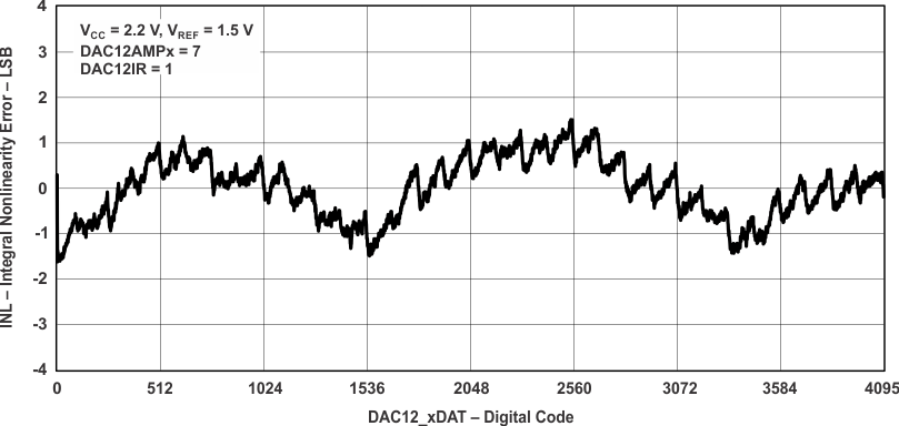
  Figure 5-27 Typical INL Error vs Digital Input Data
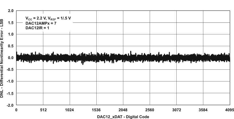
  Figure 5-28 Typical DNL Error vs Digital Input Data