SLVSCN6A November 2014 – December 2014 MSP430FR5739-EP
PRODUCTION DATA.
- 1Device Overview
- 2Revision History
- 3Pin Configuration and Functions
-
4Specifications
- 4.1 Absolute Maximum Ratings
- 4.2 Recommended Operating Conditions
- 4.3 Thermal Information
- 4.4 Active Mode Supply Current Into VCC Excluding External Current
- 4.5 Low-Power Mode Supply Currents (Into VCC) Excluding External Current
- 4.6 Schmitt-Trigger Inputs - General Purpose I/O (P1.0 to P1.7, P2.0 to P2.7, P3.0 to P3.7, P4.0 to P4.1, PJ.0 to PJ.5, RST/NMI)
- 4.7 Inputs - Ports P1 and P2 (P1.0 to P1.7, P2.0 to P2.7)
- 4.8 Leakage Current - General Purpose I/O (P1.0 to P1.7, P2.0 to P2.7, P3.0 to P3.7, P4.0 to P4.1, PJ.0 to PJ.5, RST/NMI)
- 4.9 Outputs - General Purpose I/O (P1.0 to P1.7, P2.0 to P2.7, P3.0 to P3.7, P4.0 to P4.1, PJ.0 to PJ.5)
- 4.10 Output Frequency - General Purpose I/O (P1.0 to P1.7, P2.0 to P2.7, P3.0 to P3.7, P4.0 to P4.1, PJ.0 to PJ.5)
- 4.11 Typical Characteristics - Outputs
- 4.12 Crystal Oscillator, XT1, Low-Frequency (LF) Mode
- 4.13 Crystal Oscillator, XT1, High-Frequency (HF) Mode
- 4.14 Internal Very-Low-Power Low-Frequency Oscillator (VLO)
- 4.15 DCO Frequencies
- 4.16 MODOSC
- 4.17 PMM, Core Voltage
- 4.18 PMM, SVS, BOR
- 4.19 Wake-Up from Low Power Modes
- 4.20 Timer_A
- 4.21 Timer_B
- 4.22 eUSCI (UART Mode) Recommended Operating Conditions
- 4.23 eUSCI (UART Mode)
- 4.24 eUSCI (SPI Master Mode) Recommended Operating Conditions
- 4.25 eUSCI (SPI Master Mode)
- 4.26 eUSCI (SPI Slave Mode)
- 4.27 eUSCI (I2C Mode)
- 4.28 10-Bit ADC, Power Supply and Input Range Conditions
- 4.29 10-Bit ADC, Timing Parameters
- 4.30 10-Bit ADC, Linearity Parameters
- 4.31 REF, External Reference
- 4.32 REF, Built-In Reference
- 4.33 REF, Temperature Sensor and Built-In VMID
- 4.34 Comparator_D
- 4.35 FRAM
- 4.36 JTAG and Spy-Bi-Wire Interface
-
5Detailed Description
- 5.1 Functional Block Diagram
- 5.2 CPU
- 5.3 Operating Modes
- 5.4 Interrupt Vector Addresses
- 5.5 Memory Organization
- 5.6 Bootstrap Loader (BSL)
- 5.7 JTAG Operation
- 5.8 FRAM
- 5.9 Memory Protection Unit (MPU)
- 5.10
Peripherals
- 5.10.1 Digital I/O
- 5.10.2 Oscillator and Clock System (CS)
- 5.10.3 Power Management Module (PMM)
- 5.10.4 Hardware Multiplier (MPY)
- 5.10.5 Real-Time Clock (RTC_B)
- 5.10.6 Watchdog Timer (WDT_A)
- 5.10.7 System Module (SYS)
- 5.10.8 DMA Controller
- 5.10.9 Enhanced Universal Serial Communication Interface (eUSCI)
- 5.10.10 TA0, TA1
- 5.10.11 TB0, TB1, TB2
- 5.10.12 ADC10_B
- 5.10.13 Comparator_D
- 5.10.14 CRC16
- 5.10.15 Shared Reference (REF)
- 5.10.16 Embedded Emulation Module (EEM)
- 5.10.17 Peripheral File Map
-
6Input/Output Schematics
- 6.1 Port P1, P1.0 to P1.2, Input/Output With Schmitt Trigger
- 6.2 Port P1, P1.3 to P1.5, Input/Output With Schmitt Trigger
- 6.3 Port P1, P1.6 to P1.7, Input/Output With Schmitt Trigger
- 6.4 Port P2, P2.0 to P2.2, Input/Output With Schmitt Trigger
- 6.5 Port P2, P2.3 to P2.4, Input/Output With Schmitt Trigger
- 6.6 Port P2, P2.5 to P2.6, Input/Output With Schmitt Trigger
- 6.7 Port P2, P2.7, Input/Output With Schmitt Trigger
- 6.8 Port P3, P3.0 to P3.3, Input/Output With Schmitt Trigger
- 6.9 Port P3, P3.4 to P3.6, Input/Output With Schmitt Trigger
- 6.10 Port P3, P3.7, Input/Output With Schmitt Trigger
- 6.11 Port P4, P4.0, Input/Output With Schmitt Trigger
- 6.12 Port P4, P4.1, Input/Output With Schmitt Trigger
- 6.13 Port J, J.0 to J.3 JTAG pins TDO, TMS, TCK, TDI/TCLK, Input/Output With Schmitt Trigger or Output
- 6.14 Port PJ, PJ.4 and PJ.5 Input/Output With Schmitt Trigger
- 7Device Descriptors (TLV)
-
8Device and Documentation Support
- 8.1 Device Support
- 8.2 Documentation Support
- 8.3 Community Resources
- 8.4 Trademarks
- 8.5 Electrostatic Discharge Caution
- 8.6 Glossary
- 9Mechanical Packaging and Orderable Information
パッケージ・オプション
メカニカル・データ(パッケージ|ピン)
- RHA|40
サーマルパッド・メカニカル・データ
- RHA|40
発注情報
3 Pin Configuration and Functions
3.1 Pin Diagram
Figure 3-1 shows the pin diagram for the MSP430FR5739-EP device in the 40-pin RHA package.
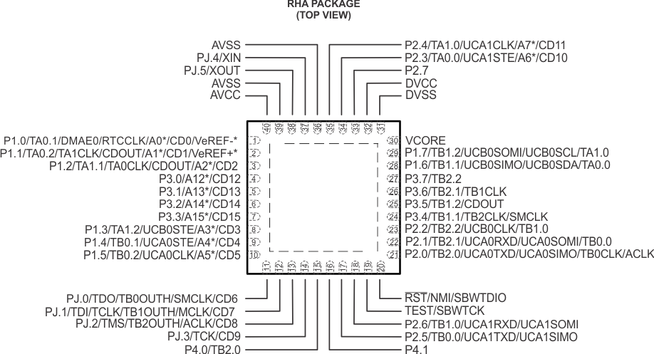
3.2 Signal Descriptions
Table 3-1 describes the signals.
Table 3-1 Signal Descriptions
| PIN | I/O (1) | DESCRIPTION | |
|---|---|---|---|
| NAME | NO. | ||
| P1.0/TA0.1/DMAE0/ RTCCLK/A0/CD0/VeREF- | 1 | I/O |
General-purpose digital I/O with port interrupt and wake up from LPMx.5 TA0 CCR1 capture: CCI1A input, compare: Out1 External DMA trigger RTC clock calibration output Analog input A0 – ADC (not available on devices without ADC) Comparator_D input CD0 External applied reference voltage (not available on devices without ADC) |
| P1.1/TA0.2/TA1CLK/ CDOUT/A1/CD1/VeREF+ | 2 | I/O |
General-purpose digital I/O with port interrupt and wake up from LPMx.5 TA0 CCR2 capture: CCI2A input, compare: Out2 TA1 input clock Comparator_D output Analog input A1 – ADC (not available on devices without ADC) Comparator_D input CD1 Input for an external reference voltage to the ADC (not available on devices without ADC) |
| P1.2/TA1.1/TA0CLK/ CDOUT/A2/CD2 | 3 | I/O |
General-purpose digital I/O with port interrupt and wake up from LPMx.5 TA1 CCR1 capture: CCI1A input, compare: Out1 TA0 input clock Comparator_D output Analog input A2 – ADC (not available on devices without ADC) Comparator_D input CD2 |
| P3.0/A12/CD12 | 4 | I/O |
General-purpose digital I/O with port interrupt and wake up from LPMx.5 Analog input A12 – ADC (not available on devices without ADC) Comparator_D input CD12 |
| P3.1/A13/CD13 | 5 | I/O |
General-purpose digital I/O with port interrupt and wake up from LPMx.5 Analog input A13 – ADC Comparator_D input CD13 |
| P3.2/A14/CD14 | 6 | I/O |
General-purpose digital I/O with port interrupt and wake up from LPMx.5 Analog input A14 – ADC (not available on devices without ADC) Comparator_D input CD14 |
| P3.3/A15/CD15 | 7 | I/O |
General-purpose digital I/O with port interrupt and wake up from LPMx.5 Analog input A15 – ADC (not available on devices without ADC) Comparator_D input CD15 |
| P1.3/TA1.2/UCB0STE/ A3/CD3 | 8 | I/O |
General-purpose digital I/O with port interrupt and wake up from LPMx.5 TA1 CCR2 capture: CCI2A input, compare: Out2 Slave transmit enable – eUSCI_B0 SPI mode Analog input A3 – ADC (not available on devices without ADC) Comparator_D input CD3 |
| P1.4/TB0.1/UCA0STE/ A4/CD4 | 9 | I/O |
General-purpose digital I/O with port interrupt and wake up from LPMx.5 TB0 CCR1 capture: CCI1A input, compare: Out1 Slave transmit enable – eUSCI_A0 SPI mode Analog input A4 – ADC (not available on devices without ADC) Comparator_D input CD4 |
| P1.5/TB0.2/UCA0CLK/ A5/CD5 | 10 | I/O |
General-purpose digital I/O with port interrupt and wake up from LPMx.5 TB0 CCR2 capture: CCI2A input, compare: Out2 Clock signal input – eUSCI_A0 SPI slave mode, Analog input A5 – ADC (not available on devices without ADC) Comparator_D input CD5 |
| PJ.0/TDO/TB0OUTH/ SMCLK/CD6 (4) | 11 | I/O |
General-purpose digital I/O Test data output port Switch all PWM outputs high impedance input – TB0 SMCLK output Comparator_D input CD6 |
| PJ.1/TDI/TCLK/TB1OUTH/ MCLK/CD7 (4) | 12 | I/O |
General-purpose digital I/O Test data input or test clock input Switch all PWM outputs high impedance input – TB1 (not available on devices without TB1) MCLK output Comparator_D input CD7 |
| PJ.2/TMS/TB2OUTH/ ACLK/CD8 (4) | 13 | I/O |
General-purpose digital I/O Test mode select Switch all PWM outputs high impedance input – TB2 (not available on devices without TB2) ACLK output Comparator_D input CD8 |
| PJ.3/TCK/CD9 (4) | 14 | I/O |
General-purpose digital I/O Test clock Comparator_D input CD9 |
| P4.0/TB2.0 | 15 | I/O |
General-purpose digital I/O with port interrupt and wake up from LPMx.5 TB2 CCR0 capture: CCI0B input, compare: Out0 (not available on devices without TB2) |
| P4.1 | 16 | I/O | General-purpose digital I/O with port interrupt and wake up from LPMx.5 |
| P2.5/TB0.0/UCA1TXD/ UCA1SIMO | 17 | I/O |
General-purpose digital I/O with port interrupt and wake up from LPMx.5 TB0 CCR0 capture: CCI0A input, compare: Out0 Transmit data – eUSCI_A1 UART mode, Slave in, master out – eUSCI_A1 SPI mode (not available on devices without UCSI_A1) |
| P2.6/TB1.0/UCA1RXD/ UCA1SOMI | 18 | I/O |
General-purpose digital I/O with port interrupt and wake up from LPMx.5 TB1 CCR0 capture: CCI0A input, compare: Out0 (not available on devices without TB1) Receive data – eUSCI_A1 UART mode, Slave out, master in – eUSCI_A1 SPI mode (not available on devices without UCSI_A1) |
| TEST/SBWTCK (4)(3) | 19 | I |
Test mode pin – enable JTAG pins Spy-Bi-Wire input clock |
| RST/NMI/SBWTDIO (4)(3) | 20 | I/O |
Reset input active low Non-maskable interrupt input Spy-Bi-Wire data input/output |
| P2.0/TB2.0/UCA0TXD/ UCA0SIMO/TB0CLK/ACLK (3) | 21 | I/O |
General-purpose digital I/O with port interrupt and wake up from LPMx.5 TB2 CCR0 capture: CCI0A input, compare: Out0 (not available on devices without TB2) Transmit data – eUSCI_A0 UART mode Slave in, master out – eUSCI_A0 SPI mode TB0 clock input ACLK output |
| P2.1/TB2.1/UCA0RXD/ UCA0SOMI/TB0.0 (3) | 22 | I/O |
General-purpose digital I/O with port interrupt and wake up from LPMx.5 TB2 CCR1 capture: CCI1A input, compare: Out1 (not available on devices without TB2) Receive data – eUSCI_A0 UART mode Slave out, master in – eUSCI_A0 SPI mode TB0 CCR0 capture: CCI0A input, compare: Out0 |
| P2.2/TB2.2/UCB0CLK/ TB1.0 | 23 | I/O |
General-purpose digital I/O with port interrupt and wake up from LPMx.5 TB2 CCR2 capture: CCI2A input, compare: Out2 (not available on devices without TB2) Clock signal input – eUSCI_B0 SPI slave mode, TB1 CCR0 capture: CCI0A input, compare: Out0 (not available on devices without TB1) |
| P3.4/TB1.1/TB2CLK/ SMCLK | 24 | I/O |
General-purpose digital I/O with port interrupt and wake up from LPMx.5 TB1 CCR1 capture: CCI1B input, compare: Out1 (not available on devices without TB1) TB2 clock input (not available on devices without TB2) SMCLK output |
| P3.5/TB1.2/CDOUT | 25 | I/O |
General-purpose digital I/O with port interrupt and wake up from LPMx.5 TB1 CCR2 capture: CCI2B input, compare: Out2 (not available on devices without TB1) Comparator_D output |
| P3.6/TB2.1/TB1CLK | 26 | I/O |
General-purpose digital I/O with port interrupt and wake up from LPMx.5 (not available on package options PW, RGE) TB2 CCR1 capture: CCI1B input, compare: Out1 (not available on devices without TB2) TB1 clock input (not available on devices without TB1) |
| P3.7/TB2.2 | 27 | I/O |
General-purpose digital I/O with port interrupt and wake up from LPMx.5 TB2 CCR2 capture: CCI2B input, compare: Out2 (not available on devices without TB2) |
| P1.6/TB1.1/UCB0SIMO/ UCB0SDA/TA0.0 | 28 | I/O |
General-purpose digital I/O with port interrupt and wake up from LPMx.5 TB1 CCR1 capture: CCI1A input, compare: Out1 (not available on devices without TB1) Slave in, master out – eUSCI_B0 SPI mode I2C data – eUSCI_B0 I2C mode TA0 CCR0 capture: CCI0A input, compare: Out0 |
| P1.7/TB1.2/UCB0SOMI/ UCB0SCL/TA1.0 | 29 | I/O |
General-purpose digital I/O with port interrupt and wake up from LPMx.5 TB1 CCR2 capture: CCI2A input, compare: Out2 (not available on devices without TB1) Slave out, master in – eUSCI_B0 SPI mode I2C clock – eUSCI_B0 I2C mode TA1 CCR0 capture: CCI0A input, compare: Out0 |
| VCORE (2) | 30 | Regulated core power supply (internal use only, no external current loading) | |
| DVSS | 31 | Digital ground supply | |
| DVCC | 32 | Digital power supply | |
| P2.7 | 33 | I/O | General-purpose digital I/O with port interrupt and wake up from LPMx.5 |
| P2.3/TA0.0/UCA1STE/ A6/CD10 | 34 | I/O |
General-purpose digital I/O with port interrupt and wake up from LPMx.5 TA0 CCR0 capture: CCI0B input, compare: Out0 Slave transmit enable – eUSCI_A1 SPI mode (not available on devices without eUSCI_A1) Analog input A6 – ADC (not available on devices without ADC) Comparator_D input CD10 |
| P2.4/TA1.0/UCA1CLK/ A7/CD11 | 35 | I/O |
General-purpose digital I/O with port interrupt and wake up from LPMx.5 TA1 CCR0 capture: CCI0B input, compare: Out0 Clock signal input – eUSCI_A1 SPI slave mode, Clock signal output – eUSCI_A1 SPI master mode (not available on devices without eUSCI_A1) Analog input A7 – ADC (not available on devices without ADC) Comparator_D input CD11 |
| AVSS | 36 | Analog ground supply | |
| PJ.4/XIN | 37 | I/O |
General-purpose digital I/O Input terminal for crystal oscillator XT1 |
| PJ.5/XOUT | 38 | I/O |
General-purpose digital I/O Output terminal of crystal oscillator XT1 |
| AVSS | 39 | Analog ground supply | |
| AVCC | 40 | Analog power supply | |
| QFN Pad | Pad | QFN package pad. Connection to VSS recommended. | |