JAJSG26C March 2016 – August 2018 MSP430FR5962 , MSP430FR5964 , MSP430FR5992 , MSP430FR5994 , MSP430FR59941
PRODUCTION DATA.
- 1デバイスの概要
- 2改訂履歴
- 3Device Comparison
- 4Terminal Configuration and Functions
-
5Specifications
- 5.1 Absolute Maximum Ratings
- 5.2 ESD Ratings
- 5.3 Recommended Operating Conditions
- 5.4 Active Mode Supply Current Into VCC Excluding External Current
- 5.5 Typical Characteristics, Active Mode Supply Currents
- 5.6 Low-Power Mode (LPM0, LPM1) Supply Currents Into VCC Excluding External Current
- 5.7 Low-Power Mode (LPM2, LPM3, LPM4) Supply Currents (Into VCC) Excluding External Current
- 5.8 Low-Power Mode (LPMx.5) Supply Currents (Into VCC) Excluding External Current
- 5.9 Typical Characteristics, Low-Power Mode Supply Currents
- 5.10 Typical Characteristics, Current Consumption per Module
- 5.11 Thermal Packaging Characteristics
- 5.12
Timing and Switching Characteristics
- 5.12.1 Power Supply Sequencing
- 5.12.2 Reset Timing
- 5.12.3 Clock Specifications
- 5.12.4 Wake-up Characteristics
- 5.12.5 Digital I/Os
- 5.12.6 LEA (Low-Energy Accelerator) (MSP430FR599x Only)
- 5.12.7 Timer_A and Timer_B
- 5.12.8 eUSCI
- 5.12.9
ADC12_B
- Table 5-23 12-Bit ADC, Power Supply and Input Range Conditions
- Table 5-24 12-Bit ADC, Timing Parameters
- Table 5-25 12-Bit ADC, Linearity Parameters
- Table 5-26 12-Bit ADC, Dynamic Performance With External Reference
- Table 5-27 12-Bit ADC, Dynamic Performance With Internal Reference
- Table 5-28 12-Bit ADC, Temperature Sensor and Built-In V1/2
- Table 5-29 12-Bit ADC, External Reference
- 5.12.10 Reference
- 5.12.11 Comparator
- 5.12.12 FRAM
- 5.12.13 Emulation and Debug
-
6Detailed Description
- 6.1 Overview
- 6.2 CPU
- 6.3 Low-Energy Accelerator (LEA) for Signal Processing (MSP430FR599x Only)
- 6.4 Operating Modes
- 6.5 Interrupt Vector Table and Signatures
- 6.6 Bootloader (BSL)
- 6.7 JTAG Operation
- 6.8 FRAM Controller A (FRCTL_A)
- 6.9 RAM
- 6.10 Tiny RAM
- 6.11 Memory Protection Unit (MPU) Including IP Encapsulation
- 6.12
Peripherals
- 6.12.1 Digital I/O
- 6.12.2 Oscillator and Clock System (CS)
- 6.12.3 Power-Management Module (PMM)
- 6.12.4 Hardware Multiplier (MPY)
- 6.12.5 Real-Time Clock (RTC_C)
- 6.12.6 Watchdog Timer (WDT_A)
- 6.12.7 System Module (SYS)
- 6.12.8 DMA Controller
- 6.12.9 Enhanced Universal Serial Communication Interface (eUSCI)
- 6.12.10 TA0, TA1, and TA4
- 6.12.11 TA2 and TA3
- 6.12.12 TB0
- 6.12.13 ADC12_B
- 6.12.14 Comparator_E
- 6.12.15 CRC16
- 6.12.16 CRC32
- 6.12.17 AES256 Accelerator
- 6.12.18 True Random Seed
- 6.12.19 Shared Reference (REF)
- 6.12.20 Embedded Emulation
- 6.13
Input/Output Diagrams
- 6.13.1 Capacitive Touch Functionality on Ports P1 to P8, and PJ
- 6.13.2 Port P1 (P1.0 to P1.2) Input/Output With Schmitt Trigger
- 6.13.3 Port P1 (P1.3 to P1.5) Input/Output With Schmitt Trigger
- 6.13.4 Port P1 (P1.6 and P1.7) Input/Output With Schmitt Trigger
- 6.13.5 Port P2 (P2.0 to P2.2) Input/Output With Schmitt Trigger
- 6.13.6 Port P2 (P2.3 and P2.4) Input/Output With Schmitt Trigger
- 6.13.7 Port P2 (P2.5 and P2.6) Input/Output With Schmitt Trigger
- 6.13.8 Port P2 (P2.7) Input/Output With Schmitt Trigger
- 6.13.9 Port P3 (P3.0 to P3.3) Input/Output With Schmitt Trigger
- 6.13.10 Port P3 (P3.4 to P3.7) Input/Output With Schmitt Trigger
- 6.13.11 Port P4 (P4.0 to P4.3) Input/Output With Schmitt Trigger
- 6.13.12 Port P4 (P4.4 to P4.7) Input/Output With Schmitt Trigger
- 6.13.13 Port P5 (P5.0 to P5.7) Input/Output With Schmitt Trigger
- 6.13.14 Port P6 (P6.0 to P6.7) Input/Output With Schmitt Trigger
- 6.13.15 Port P7 (P7.0 to P7.3) Input/Output With Schmitt Trigger
- 6.13.16 Port P7 (P7.4 to P7.7) Input/Output With Schmitt Trigger
- 6.13.17 Port P8 (P8.0 to P8.3) Input/Output With Schmitt Trigger
- 6.13.18 Port PJ (PJ.4 and PJ.5) Input/Output With Schmitt Trigger
- 6.13.19 Port PJ (PJ.6 and PJ.7) Input/Output With Schmitt Trigger
- 6.13.20 Port PJ (PJ.0 to PJ.3) JTAG Pins TDO, TMS, TCK, TDI/TCLK, Input/Output With Schmitt Trigger
- 6.14 Device Descriptors (TLV)
- 6.15 Memory Map
- 6.16 Identification
- 7Applications, Implementation, and Layout
- 8デバイスおよびドキュメントのサポート
- 9メカニカル、パッケージ、および注文情報
パッケージ・オプション
メカニカル・データ(パッケージ|ピン)
サーマルパッド・メカニカル・データ
- RGZ|48
発注情報
7.1.3 JTAG
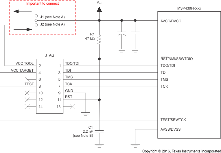
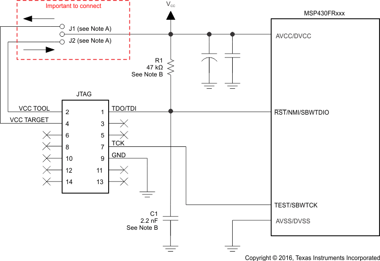
With the proper connections, the debugger and a hardware JTAG interface (such as the MSP-FET or MSP-FET430UIF) can be used to program and debug code on the target board. In addition, the connections also support the MSP-GANG production programmers, thus providing an easy way to program prototype boards, if desired. Figure 7-3 shows the connections between the 14-pin JTAG connector and the target device required to support in-system programming and debugging for 4-wire JTAG communication. Figure 7-4 shows the connections for 2-wire JTAG mode (Spy-Bi-Wire).
The connections for the MSP-FET and MSP-FET430UIF interface modules and the MSP-GANG are identical. Both can supply VCC to the target board (through pin 2). In addition, the MSP-FET and MSP-FET430UIF interface modules and MSP-GANG have a VCC sense feature that, if used, requires an alternate connection (pin 4 instead of pin 2). The VCC-sense feature senses the local VCC present on the target board (that is, a battery or other local power supply) and adjusts the output signals accordingly. Figure 7-3 and Figure 7-4 show a jumper block that supports both scenarios of supplying VCC to the target board. If this flexibility is not required, the desired VCC connections may be hard-wired to eliminate the jumper block. Pins 2 and 4 must not be connected at the same time.
For additional design information regarding the JTAG interface, see the MSP430 Hardware Tools User’s Guide.

