SLOS075J November 1979 – January 2015 NE5532 , NE5532A , SA5532 , SA5532A
PRODUCTION DATA.
- 1 Features
- 2 Applications
- 3 Description
- 4 Simplified Schematic
- 5 Revision History
- 6 Pin Configuration and Functions
- 7 Specifications
- 8 Detailed Description
- 9 Application and Implementation
- 10Power Supply Recommendations
- 11Layout
- 12Device and Documentation Support
- 13Mechanical, Packaging, and Orderable Information
パッケージ・オプション
メカニカル・データ(パッケージ|ピン)
サーマルパッド・メカニカル・データ
発注情報
9 Application and Implementation
NOTE
Information in the following applications sections is not part of the TI component specification, and TI does not warrant its accuracy or completeness. TI’s customers are responsible for determining suitability of components for their purposes. Customers should validate and test their design implementation to confirm system functionality.
9.1 Typical Application
Some applications require differential signals. Figure 4 shows a simple circuit to convert a single-ended input of 2 V to 10 V into differential output of ±8 V on a single 15-V supply. The output range is intentionally limited to maximize linearity. The circuit is composed of two amplifiers. One amplifier acts as a buffer and creates a voltage, VOUT+. The second amplifier inverts the input and adds a reference voltage to generate VOUT–. Both VOUT+ and VOUT– range from 2 V to 10 V. The difference, VDIFF, is the difference between VOUT+ and VOUT–.
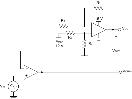 Figure 4. Schematic for Single-Ended Input to Differential Output Conversion
9.1.1 Design Requirements
The design requirements are as follows:
- Supply voltage: 15 V
- Reference voltage: 12V
- Input: 2 V to 10 V
- Output differential: ±8 V
9.1.2 Detailed Design Procedure
The circuit in Figure 4 takes a single-ended input signal, VIN, and generates two output signals, VOUT+ and VOUT– using two amplifiers and a reference voltage, VREF. VOUT+ is the output of the first amplifier and is a buffered version of the input signal, VINEquation 1. VOUT– is the output of the second amplifier which uses VREF to add an offset voltage to VIN and feedback to add inverting gain. The transfer function for VOUT– is Equation 2.
The differential output signal, VDIFF, is the difference between the two single-ended output signals, VOUT+ and VOUT–. Equation 3 shows the transfer function for VDIFF. By applying the conditions that R1 = R2 and R3 = R4, the transfer function is simplified into Equation 6. Using this configuration, the maximum input signal is equal to the reference voltage and the maximum output of each amplifier is equal to the VREF. The differential output range is 2×VREF. Furthermore, the common mode voltage will be one half of VREF (see Equation 7).

9.1.2.1 Amplifier Selection
Linearity over the input range is key for good dc accuracy. The common mode input range and the output swing limitations determine the linearity. In general, an amplifier with rail-to-rail input and output swing is required. Bandwidth is a key concern for this design. Since the NE5532 has a bandwidth of 10 MHz, this circuit will only be able to process signals with frequencies of less than 10 MHz.
9.1.2.2 Passive Component Selection
Because the transfer function of VOUT– is heavily reliant on resistors (R1, R2, R3, and R4), use resistors with low tolerances to maximize performance and minimize error. This design used resistors with resistance values of 36 kΩ with tolerances measured to be within 2%. But, if the noise of the system is a key parameter, the user can select smaller resistance values (6 kΩ or lower) to keep the overall system noise low. This ensures that the noise from the resistors is lower than the amplifier noise.
9.1.3 Application Curves
The measured transfer functions in Figure 5, Figure 6, and Figure 7 were generated by sweeping the input voltage from 0 V to 12V. However, this design should only be used between 2 V and 10 V for optimum linearity.
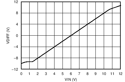 Figure 5. Differential Output Voltage vs Input Voltage
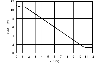 Figure 7. Positive Output Voltage Node vs Input Voltage
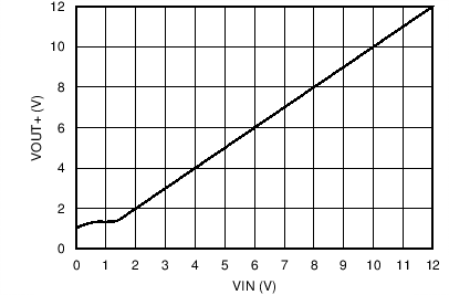 Figure 6. Positive Output Voltage Node vs Input Voltage